Chip manufacturing method

A manufacturing method and chip technology, applied in the field of chip manufacturing, can solve problems such as reduced productivity, poor processing, and crystal orientation changes, and achieve the effects of suppressing abnormal elongation, reducing the number of inversions, and reliable segmentation

Pending Publication Date: 2022-07-29
DISCO CORP
View PDF1 Cites 0 Cited by
  • Summary
  • Abstract
  • Description
  • Claims
  • Application Information

AI Technical Summary

Problems solved by technology

[0006] However, when laser processing grooves are formed on a laminate, the crystal orientation of a part of the substrate near the bottom of the processing groove may change due to the thermal influence of the laser beam on the front side of the substrate.
[0007] The extending direction of the crack extending from the modified layer depends on the crystal orientation of the substrate. Therefore, when the crystal orientation changes, there is a problem that the crack is formed on the front surface of the substrate so as to avoid the laser-processed groove. Exposed, wafer cannot be divided along the spacer (ie, processing failure occurs)
[0009] However, after the modified layer is formed by exposing the back surface of the wafer upward, the laser processing groove is formed by exposing the front surface of the wafer upward, and then the substrate needs to be ground by exposing the back surface of the wafer upward again. During the period from the formation of the modified layer to the grinding, it is necessary to perform at least two operations of turning the front and back of the wafer, so the productivity is reduced

Method used


Image

  • Chip manufacturing method
  • Chip manufacturing method
  • Chip manufacturing method

Examples


no. 2 Embodiment approach

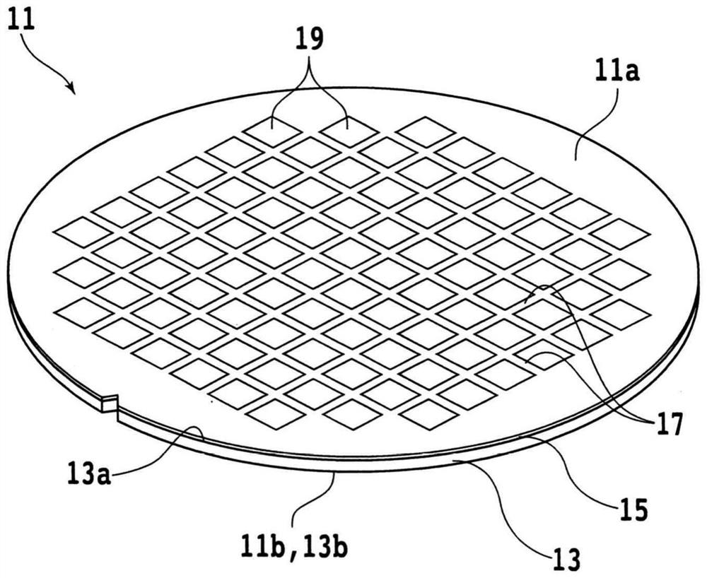
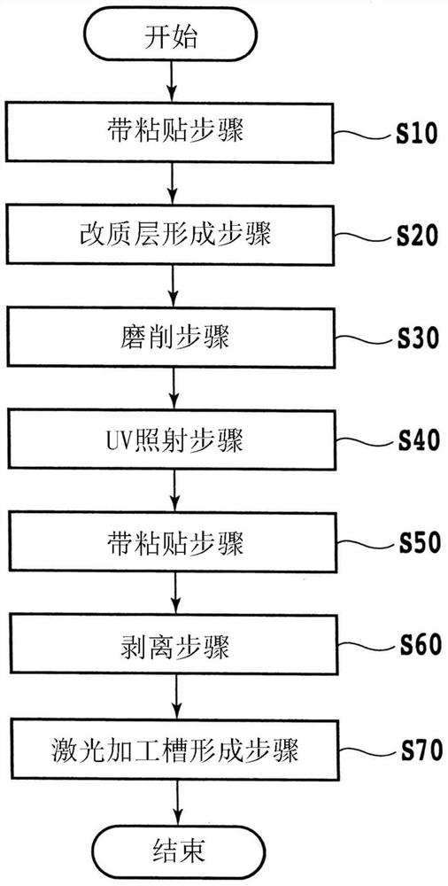
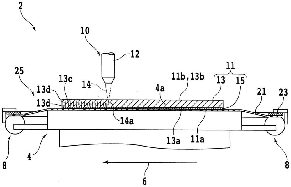
[0128] Next, the second embodiment will be described. Figure 12 It is a flowchart of the manufacturing method of the device chip 35 of 2nd Embodiment. In the laser processing groove forming step S70 of the second embodiment, as Figure 13 As shown, a laser-machined groove 15a having a predetermined depth that does not completely break the laminated body 15 is formed. 4 .

[0129] Figure 13 is one laser-machined groove 15a that does not reach the front surface 13a of the substrate 13 4 An enlarged cross-sectional view of the wafer 11 . For example, the laser processing groove 15a can be formed by reducing the average output, the repetition frequency, increasing the processing feed rate, or changing the height position of the light-converging point 50a. 4 .

[0130] By forming laser processing grooves 15a that do not reach the front surface 13a 4 , the damage on the front surface 13a side of the substrate 13 in the laser processing groove forming step S70 can be reduced...


PUM


Abstract

The invention provides a method for manufacturing a chip, which can reliably divide a wafer by inhibiting abnormal extension of cracks and can reduce the number of times that the front surface and the back surface of the wafer are turned over. The chip manufacturing method comprises the following steps: a modified layer forming step of irradiating a first laser beam along a division predetermined line in a state that the back side of a substrate in a wafer having the substrate and a laminated body is exposed and the focal point of the first laser beam having a wavelength penetrating through the substrate is positioned in the substrate from the back side of the substrate, forming a modified layer and cracks; a grinding step of grinding the back surface side of the substrate exposed in the modified layer forming step after the modified layer forming step to thin the wafer to a predetermined thickness; and a laser processing groove forming step of irradiating a second laser beam having a wavelength absorbed by the substrate from the front surface side of the wafer along the division predetermined line after the grinding step, and forming a laser processing groove in the laminated body.

Description

technical field [0001] The present invention relates to a method of manufacturing a chip by dividing a wafer in which a substrate and a laminate are laminated to manufacture a chip. Background technique [0002] A semiconductor chip is usually a wafer having a substrate formed of a semiconductor such as silicon and a laminate such as a Low-k film and a conductive layer formed on the front surface of the substrate along a spacer (segmentation plan) set on the front surface of the substrate. line) is produced by dividing a wafer. In addition, TEGs (Test Element Groups) may be formed in some regions of the spacers in the laminate. [0003] In order to divide the wafer along the lanes, for example, first, a pulsed laser beam having a wavelength absorbed by the substrate and the laminate is irradiated along the lanes to form laser processing grooves along the lanes. The laminated body was partially removed by the laser processing groove, and the front surface of the substrate w...

Claims


Application Information

Patent Timeline
Patent Type & Authority Applications(China)
IPC IPC(8): H01L21/78H01L21/268B23K26/364
CPCH01L21/78H01L21/2683B23K26/364H01L21/6836H01L2221/68327H01L2221/6834H01L2221/68336H01L21/304H01L21/3043H01L21/268
Inventor 桥本一辉
Owner DISCO CORP
Why Eureka
Try Eureka