
A Vertical Double Diffused Metal Oxide Semiconductor Field Effect Transistor

A technology of oxide semiconductors and field effect transistors, which is applied in the field of vertical double-diffused metal oxide semiconductor field effect transistors, can solve the problems of device threshold voltage drift, threshold voltage drift failure, etc., to reduce the number of holes and slow down the threshold voltage Drift, the effect of reducing degradation effects

Active Publication Date: 2019-06-14
北京中科微投资管理有限责任公司
View PDF4 Cites 0 Cited by
  • Summary
  • Abstract
  • Description
  • Claims
  • Application Information

AI Technical Summary

Problems solved by technology

[0005] By providing a vertical double-diffused metal oxide semiconductor field effect transistor, the present invention solves the problem that VDMOS in the prior art requires a thicker gate oxide thickness to meet the voltage requirements, but a thicker gate oxide layer will accelerate the radiation of the device. The drift of the threshold voltage during the illumination causes the technical problem that the threshold voltage drift is prone to failure

Method used


Image

  • A Vertical Double Diffused Metal Oxide Semiconductor Field Effect Transistor
  • A Vertical Double Diffused Metal Oxide Semiconductor Field Effect Transistor
  • A Vertical Double Diffused Metal Oxide Semiconductor Field Effect Transistor

Examples


Embodiment Construction

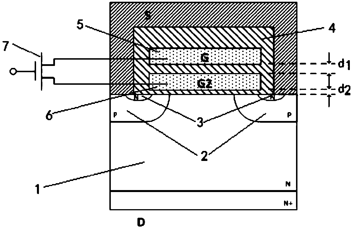
[0022] The embodiments of the present application provide a vertical double-diffused metal-oxide-semiconductor field effect transistor, which solves the problem that the VDMOS in the prior art requires a thicker gate oxide layer thickness to meet the voltage requirements, but the thicker gate oxide layer will accelerate the device. The drift of the threshold voltage when exposed to irradiation leads to the technical problem of failure of the threshold voltage drift. The technical effect of slowing down threshold voltage drift and improving reliability is realized.

[0023] In order to solve the above-mentioned technical problems, the general idea of ​​the technical solutions provided by the embodiments of the present application is as follows:

[0024] The present application provides a vertical double-diffused metal-oxide-semiconductor field effect transistor, the transistor comprising:

[0025] Substrate, P well region, N well region, gate oxide layer and gate;

[0026] Wh...


PUM


Abstract

The invention discloses a vertical double diffused metallic oxide semiconductor field effect transistor. The vertical double diffused metallic oxide semiconductor field effect transistor comprises a substrate, a P well region, an N well region, gate oxide layers and grid electrodes, wherein the grid electrodes comprise a first grid electrode and a second grid electrode; the second grid electrode is positioned between the first grid electrode and the substrate; the thickness of the gate oxide layer between the first grid electrode and the second grid electrode is a first thickness; the thickness of the gate oxide layer between the second grid electrode and the substrate is a second thickness; and the second grid electrode is connected with a refresh structure through a switch so that the second grid electrode can be refreshed to an initial potential. The transistor provided by the invention solves the technical problem that a threshold voltage drift failure easily occurs due to the fact that a VDMOS in the prior art needs the gate oxide layers with relatively high thicknesses to meet voltage requirements but the relatively thick gate oxide layers can accelerate the drift of threshold voltage when the device is subjected to radiation. The technical effects of slowing down the threshold voltage drift and improving the reliability are reached.

Description

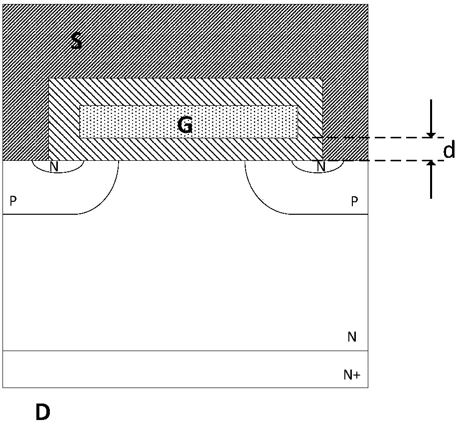
technical field [0001] The present invention relates to the field of semiconductors, in particular to a vertical double diffused metal oxide semiconductor field effect transistor (Vertical Diffuse Metal Oxide Semiconductor Field Effect Transistor, VDMOSFET). Background technique [0002] In the field of power semiconductors, such as figure 1 As shown, a vertical metal oxide semiconductor field effect transistor (Metal Oxide Semiconductor Field Effect Transistor, MOSFET) formed by a vertical double diffusion process is called a VDMOSFET, or VDMOS for short. Because this type of device usually needs to form a relatively large voltage between the gate G and the silicon substrate, the gate oxide thickness d is relatively thicker than that of a MOSFET device for logic applications. [0003] When a VDMOS device is used in space, it will be continuously exposed to ionizing radiation (such as X-rays and gamma rays, etc.), thereby resulting in a total dose effect (Total Ionizing Dos...

Claims


Application Information

Patent Timeline
Patent Type & Authority Patents(China)
IPC IPC(8): H01L29/78H01L29/423
CPCH01L29/4232H01L29/7831
Inventor 孙博韬王立新单尼娜
Owner 北京中科微投资管理有限责任公司
Learn More