IGBT structure with trench emitter buried layer
An emitter and trench technology, applied in the direction of electrical components, circuits, semiconductor devices, etc., to achieve the effect of suppressing dynamic avalanche, suppressing dynamic avalanche breakdown, and suppressing EMI noise interference
- Summary
- Abstract
- Description
- Claims
- Application Information
AI Technical Summary
Problems solved by technology
Method used
Image
Examples
Embodiment Construction
[0013] The specific embodiments of the present invention are described below so that those skilled in the art can understand the present invention, but it should be clear that the present invention is not limited to the scope of the specific embodiments. For those of ordinary skill in the art, as long as various changes Within the spirit and scope of the present invention defined and determined by the appended claims, these changes are obvious, and all inventions and creations using the concept of the present invention are included in the protection list.
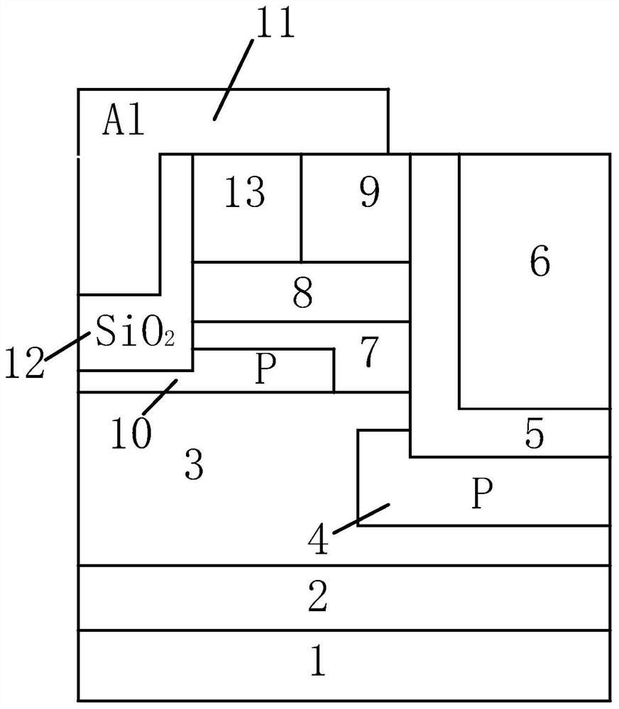
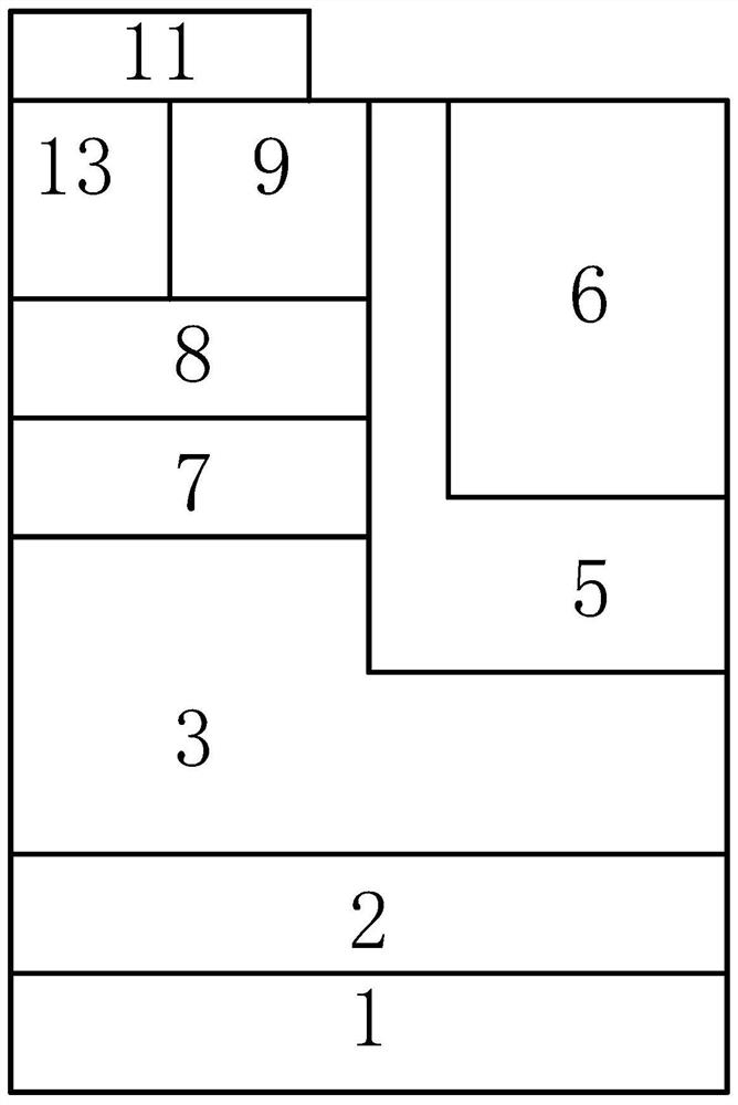
[0014] The present invention proposes a novel IGBT structure with a trench emitter buried layer, the cell structure of which is as follows figure 1 As shown, it includes a P-type collector region (1), an N-type buffer layer (2) above the collector region (1) and an N-type drift region (3), and a polysilicon gate is arranged in the drift region (3). Electrode (6) and gate oxide layer (5), metal emitter (11) and emitter oxide...
PUM
 Abstract
Description
Claims
Application Information

