
Local soi LDMOS device for frequency boosting overcoming short channel effect

A short-channel effect and frequency technology, which is applied in the direction of semiconductor devices, electrical components, circuits, etc., can solve the problems that the deterioration of short-channel characteristics cannot be suppressed, and the frequency characteristics cannot be realized, so as to achieve the suppression of short-channel effects and good short-circuit Channel characteristics, effect of guaranteed breakdown voltage

Active Publication Date: 2017-10-17
UNIV OF ELECTRONICS SCI & TECH OF CHINA
View PDF4 Cites 0 Cited by
  • Summary
  • Abstract
  • Description
  • Claims
  • Application Information

AI Technical Summary

Problems solved by technology

However, the variable doping structure in the drift region cannot suppress the deterioration of short channel characteristics brought about by the reduction of device feature size, nor can it achieve a significant improvement in frequency characteristics.

Method used


Image

  • Local soi LDMOS device for frequency boosting overcoming short channel effect
  • Local soi LDMOS device for frequency boosting overcoming short channel effect
  • Local soi LDMOS device for frequency boosting overcoming short channel effect

Examples


Embodiment

[0043] This example is aimed at Figure 4 The ET-PSOI LDMOS device shown adopts a local SOI structure BOX layer directly below the channel region. The shape of the BOX layer is rectangular, and the top corner of the BOX layer near the drift region is passivated into a chamfered structure to reduce the electric field at the sharp corner of the BOX layer. Increase breakdown voltage while improving cutoff frequency and drive capability.

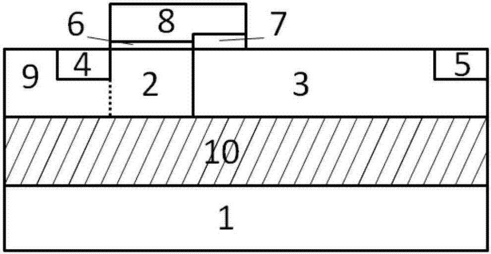
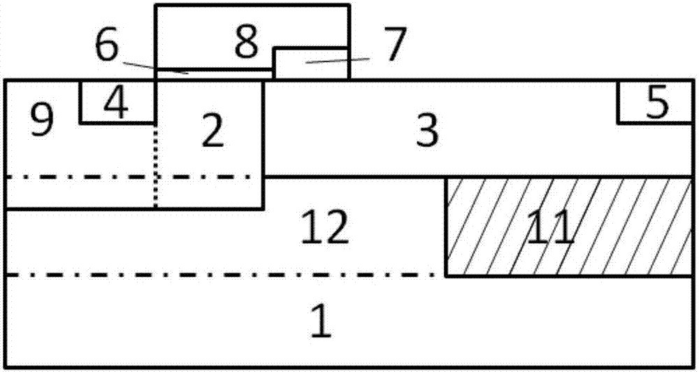
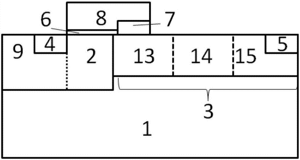
[0044] The small-sized LDMOS device with local ultra-thin SOI in this embodiment includes a semiconductor substrate 1, a channel region 2, a drift region 3, a source region 4, a drain region 5, a gate oxide 6, a field oxide 7, a gate 8, a trench The channel substrate heavily doped region 9, the BOX layer 18, the side wall 19, and the source extension region 20, wherein the BOX layer 18 is a rectangle with a thickness of 30nm, located directly below the channel region and having the same length as the channel region, The distance between the upp...


PUM


Abstract

The invention discloses a local ultra-thin SOI LDMOS device which overcomes the short channel effect and increases the frequency, and belongs to the field of semiconductor devices. Including semiconductor substrate 1, channel region 2, drift region 3, source region 4, drain region 5, gate oxide 6, field oxygen 7, gate 8, channel substrate heavily doped region 9, BOX layer 18, sidewall 19. The source extension region 20, wherein the drift region 3 is a lateral variable doping structure, characterized in that a through groove is opened along the width direction of the drift region at one end of the BOX layer close to the drift region, and the BOX layer 18 is located at the side of the channel Directly below, or directly below the channel and part of the source region, or directly below the channel and the source region, to ensure the breakdown voltage while improving the frequency characteristics and drive capability of the device. The invention effectively suppresses the short-channel effect, and improves the frequency characteristic and driving ability while ensuring the breakdown voltage.

Description

technical field [0001] The invention belongs to the field of semiconductor devices and relates to a small-sized laterally diffused metal oxide semiconductor field effect transistor (LDMOS), in particular to a local ultra-thin SOI LDMOS device which overcomes the short channel effect and improves the cut-off frequency. Background technique [0002] The rapid development of wireless communication systems, power switch modules and related technologies promotes the rapid development of power integrated circuits. As the operating frequency becomes higher and higher, the requirements for circuit and device frequency are getting higher and higher. In RF power devices, LDMOS (Laterally Diffused Metal Oxide Semiconductor Field Effect Transistor) devices play an important role in RF power devices due to their good process compatibility and excellent performance. [0003] SOI RF LDMOS devices are widely used in the radio frequency field because of their good electrical insulation, low ...

Claims


Application Information

Patent Timeline
Patent Type & Authority Patents(China)
IPC IPC(8): H01L29/78H01L29/06
CPCH01L29/0649H01L29/7824
Inventor 王向展邹淅张易黄建国赵迪于奇刘洋
Owner UNIV OF ELECTRONICS SCI & TECH OF CHINA
Learn More