A kind of insulated gate bipolar transistor and its manufacturing method
A bipolar transistor and insulated gate technology, which is applied in semiconductor/solid-state device manufacturing, semiconductor devices, electrical components, etc., can solve the problem of not being able to guarantee the breakdown voltage of the device at the same time, the forward conducting voltage drop of the device, and the dielectric layer withstand voltage of the feedback capacitor gate performance and reliability issues
- Summary
- Abstract
- Description
- Claims
- Application Information
AI Technical Summary
Problems solved by technology
Method used
Image
Examples
Embodiment 1
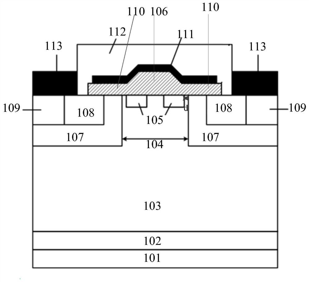
[0042] This embodiment provides an insulated gate bipolar transistor, such as figure 1 As shown, the insulated gate bipolar transistor includes: a substrate 101; a buffer layer 102, an epitaxial layer 103, a JFET region 104, a CJI doped region 105, and a first gate dielectric layer 106; wherein,
[0043] The substrate 101 is a SiC substrate of the first heavily doped type, and the first heavily doped type may be N-type or P-type, and the substrate 101 in this embodiment may be an N-type SiC substrate or a P-type SiC substrate with a doping concentration of 10 18 ~10 19 cm -3 .
[0044] The buffer layer 102 is a SiC buffer layer of the second doping type, epitaxially formed on the substrate 101; the second doping type can be P-type or N-type, and the buffer layer 102 in this embodiment is a P-type SiC buffer layer. The doping level and thickness of the buffer layer 102 can be specifically set according to the breakdown voltage, forward voltage drop and dynamic characteristi...
Embodiment 2
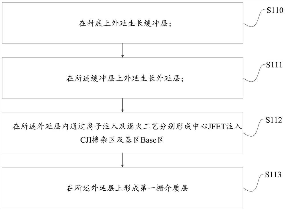
[0062] Corresponding to Embodiment 1, this embodiment provides a method for manufacturing an insulated gate bipolar transistor, such as figure 2 As shown, the methods include:
[0063] S110, epitaxially growing a buffer layer on the substrate;
[0064] In this embodiment, the substrate is a SiC substrate of the first heavily doped type, and the first heavily doped type can be N-type or P-type, and the substrate in this embodiment can be an N-type SiC substrate, or can be P-type SiC substrate with a doping concentration of 10 18 ~10 19 cm -3 .
[0065] The buffer layer is a SiC buffer layer of the second doping type, epitaxially formed on the substrate; the second doping type can be P-type or N-type, and the buffer layer in this embodiment is a P-type SiC buffer layer. The doping level and thickness of the buffer layer can be specifically set according to the breakdown voltage, forward conduction voltage drop and dynamic characteristics of the transistor device. Dynamic ...
PUM
| Property | Measurement | Unit |
|---|---|---|
| thickness | aaaaa | aaaaa |
| width | aaaaa | aaaaa |
| width | aaaaa | aaaaa |
Abstract
Description
Claims
Application Information

