A kind of LED chip with ito film structure and preparation method thereof

A technology of LED chip and thin film structure, which is applied in the direction of electrical components, circuits, semiconductor devices, etc., can solve problems such as the influence of pad performance on chip reliability, ITO film shedding, and abnormal shedding of metal electrode layer 106, etc., to improve the bonding wire. Reliability and luminous efficiency, stable working voltage, improved adhesion and integrity effects

Active Publication Date: 2018-08-28
NANCHANG KAIXUN PHOTOELECTRIC CO LTD
View PDF6 Cites 0 Cited by
  • Summary
  • Abstract
  • Description
  • Claims
  • Application Information

AI Technical Summary

Problems solved by technology

In practical applications, a layer of ITO film is grown on the p-GaP window layer 105, and then the metal electrode layer 106 is deposited to be used as a pad material. In the bonding wire test to the pad, it is found that the ITO film is easy to fall off, The problem of abnormal shedding of the metal electrode layer 106 has seriously affected its pad performance and chip reliability

Method used


Image

  • A kind of LED chip with ito film structure and preparation method thereof
  • A kind of LED chip with ito film structure and preparation method thereof
  • A kind of LED chip with ito film structure and preparation method thereof

Examples


Embodiment Construction

[0028] The present invention will be further described in detail below in conjunction with the embodiments and the accompanying drawings.

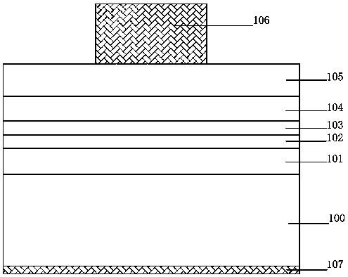
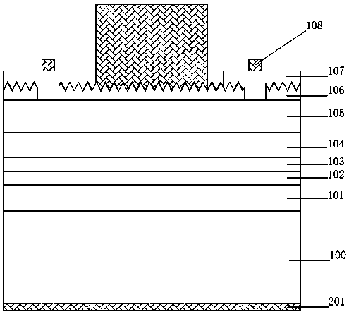
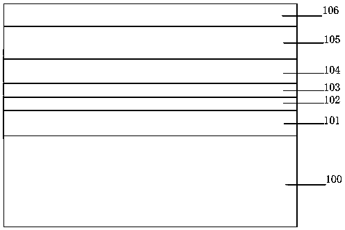
[0029] An LED chip with ITO film structure, such as figure 2 As shown, a GaAs substrate 100 is included. A buffer layer 101, an n-AlGaInP confinement layer 102, an MQW multiple quantum well active layer 103, a p-AlGaInP confinement layer 104, and a p-GaP window are sequentially arranged on the GaAs substrate 100. Layer 105 and AlGaInP roughened layer 106. AlGaInP roughened layer 106 is a patterned AlGaInP roughened layer. An ITO thin film contact layer 107 is provided on the patterned AlGaInP roughened layer 106, and an ITO thin film contact layer 107 is provided The patterned ITO thin film contact layer is provided with a metal electrode layer 108 on the patterned ITO thin film contact layer, and a back electrode layer 201 is provided under the GaAs substrate 100. The metal electrode layer 108 includes a main electrode and an extended electr...


PUM


Abstract

The invention discloses an LED chip having an ITO thin film structure and a manufacturing method therefor. The LED chip comprises a GaAs substrate; a buffer layer, an n-AIGaInP limiting layer, an MQW multiple quantum well active layer, a p-AIGaInP limiting layer, a p-GaP window layer and an AIGaInP coarsened layer are orderly arranged on the GaAs substrate; an ITO thin film layer is arranged on the patterned AIGaInP coarsened layer, a patterned ITO thin film contact layer is arranged on the ITO thin film layer, a metal electrode layer is arranged on the patterned ITO thin film contact layer, and a back electrode layer is arranged below the GaAs substrate. The LED chip is characterized in that the metal electrode layer comprises a main electrode and an expansion electrode, the main electrode is connected onto the patterned AIGaInP coarsened layer, and the expansion electrode is connected onto the ITO thin film layer. According to the LED chip and the manufacturing method therefor, adhesiveness and completeness of the whole metal electrode layer are improved, working voltage stability of a light emitting diode can be ensured, reliability and light emitting efficiency of welding wires of products can be improved, and product quality and yield rates can be greatly enhanced.

Description

Technical field [0001] The invention relates to the field of semiconductor light-emitting diodes, in particular to an LED chip with an ITO film structure and a preparation method thereof. Background technique [0002] Light-emitting diodes (LEDs) have the advantages of high luminous efficiency, low energy consumption, long life, high safety, and high environmental protection. It is a lighting method with broad application prospects and has attracted more and more countries’ attention. At present, LEDs have been widely used In the field of high-efficiency solid-state lighting, such as display screens, automotive lights, backlights, traffic lights, landscape lighting, etc. [0003] Such as figure 1 As shown, the conventional AlGaInP light-emitting diode includes a GaAs substrate 100, a buffer layer 101, an n-AIGaInP confinement layer 102, an MQW multiple quantum well active layer 103, a p-AIGaInP confinement layer 104 and a p-GaP window layer 105, and a metal electrode layer 106 is ...

Claims


Application Information

Patent Timeline
Patent Type & Authority Patents(China)
IPC IPC(8): H01L33/06H01L33/22H01L33/62H01L33/00
CPCH01L33/005H01L33/06H01L33/22H01L33/36H01L33/62
Inventor 张银桥潘彬
Owner NANCHANG KAIXUN PHOTOELECTRIC CO LTD
Why Eureka
Try Eureka