A kind of LED chip with ITO film structure and preparation method thereof

A LED chip and thin film structure technology, applied in the direction of electrical components, circuits, semiconductor devices, etc., can solve the problems of metal electrode layer shedding, metal electrode layer pad performance AlGaInP-based chip reliability, ITO film layer shedding and other problems, Achieve the effects of reducing contact voltage, improving adhesion and integrity, and improving reliability of welding wires

Active Publication Date: 2018-05-29
NANCHANG KAIXUN PHOTOELECTRIC CO LTD
View PDF5 Cites 0 Cited by
  • Summary
  • Abstract
  • Description
  • Claims
  • Application Information

AI Technical Summary

Problems solved by technology

In practical applications, a layer of ITO film layer is grown on the GaP layer first, and then the metal electrode layer used as the pad material is deposited. However, it is found in the bonding wire test of the pad that the ITO film layer is prone to fall off, The abnormal phenomenon that the metal electrode layer falls off, which will seriously affect the pad performance of the metal electrode layer and the reliability of AlGaInP-based chips

Method used


Image

  • A kind of LED chip with ITO film structure and preparation method thereof
  • A kind of LED chip with ITO film structure and preparation method thereof
  • A kind of LED chip with ITO film structure and preparation method thereof

Examples


Embodiment Construction

[0027] The present invention will be described in further detail below in conjunction with the embodiments and with reference to the accompanying drawings.

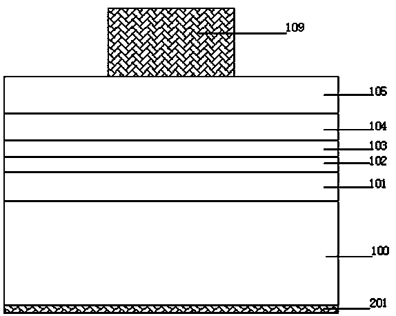
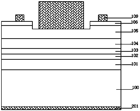
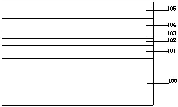
[0028] A kind of LED chip with ITO film structure, such as figure 2 As shown, a GaAs substrate 100 is included, and a buffer layer 101, an n-AlGaInP confinement layer 102, a multi-quantum well active layer 103, a p-AlGaInP confinement layer 104, and a p-GaP window layer are sequentially arranged on the GaAs substrate 100 105, an ITO film layer 106 is provided on the p-GaP window layer 105, a metal electrode layer 109 is provided on the ITO film layer 106, and a back electrode 201 is made under the GaAs substrate 100; the metal electrode layer 109 includes a main electrode and a For the extended electrodes, the main electrode is connected to the p-GaP window layer 105 , and the extended electrode is connected to the ITO thin film layer 106 .

[0029] A kind of preparation method of LED chip with ITO film structure, concr...


PUM

PropertyMeasurementUnit
diameteraaaaaaaaaa
lengthaaaaaaaaaa
widthaaaaaaaaaa

Abstract

The invention discloses an LED chip with an ITO thin film structure and a preparation method of the LED chip, and belongs to the field of semiconductor light-emitting diodes. The method comprises the following steps: firstly, fabricating an epitaxial wafer of the light-emitting diode; fabricating a patterned dielectric film layer on the epitaxial wafer and fabricating the patterned ITO thin film layer and p-GaP window layer in an etching manner; and fabricating a metal electrode layer on the patterned ITO thin film layer and p-GaP window layer. The metal electrode layer comprises a main electrode and an extended electrode. The patterned ITO thin film layer and p-GaP window layer are adopted as contact layers; and the main electrode as a bonding pad is connected to the p-GaP window layer; and the extended electrode is connected to the ITO thin film layer. The adhesiveness of the overall metal electrode layer is improved; a stable working voltage of a light-emitting device is ensured; the bonding wire reliability of a product is improved; and the quality and the yield of the product are greatly improved.

Description

technical field [0001] The invention relates to the field of semiconductor light emitting diodes, in particular to an LED chip with an ITO thin film structure and a preparation method thereof. Background technique [0002] LED has the advantages of high light efficiency, low energy consumption, long life, high safety, and high environmental protection. It is a lighting method with broad application prospects, and has been valued by more and more countries. At present, LEDs have been widely used in the field of high-efficiency solid-state lighting, such as display screens, automotive lights, backlights, traffic lights, and landscape lighting. [0003] Such as figure 1 As shown, a conventional AlGaInP light-emitting diode includes a GaAs substrate 100, a buffer layer 101, an n-AlGaInP confinement layer 102, an MQW multi-quantum well active layer 103, a p-AlGaInP confinement layer 104, and a p-GaP window layer 105, and a metal electrode layer 109 is directly disposed on the p...

Claims


Application Information

Patent Timeline
Patent Type & Authority Patents(China)
IPC IPC(8): H01L33/38H01L33/00
CPCH01L33/0062H01L33/387H01L2933/0016
Inventor 张银桥潘彬
Owner NANCHANG KAIXUN PHOTOELECTRIC CO LTD
Why Eureka
Try Eureka