Interferometer error calibrating device and method

An error calibration and interferometer technology, which is applied in the field of interferometer error calibration devices, can solve the problems that the factors affected by the interferometer cannot be measured in real time, there are differences in the influence of the environment, the installation error of the interferometer, etc., so as to reduce the impact, Increase the assembly error test and improve the effect of assembly and adjustment accuracy

Active Publication Date: 2016-11-23
SHANGHAI MICRO ELECTRONICS EQUIP (GRP) CO LTD
View PDF5 Cites 4 Cited by
  • Summary
  • Abstract
  • Description
  • Claims
  • Application Information

AI Technical Summary

Problems solved by technology

Since the position measurement of the moving table usually uses a laser interferometer, and for the laser interferometer measurement system, the laser is greatly affected by the environment such as temperature and pressure. The direction of propagation will change, resulting in a measurement error in position
Especially when the stroke of the test bench is large, it is difficult for the ambient air bath to control the temperature and pressure in the whole stroke, and as the distance between the two measuring axes of the interferometer increases, the two measuring axes are affected by the environment there are also differences
At present, in the integration process of the lithography machine, only the installation error of the interferometer, such as Abbe error and cosine error, has been calibrated, but the factors affected by the environment of the interferometer cannot be measured in real time

Method used


Image

  • Interferometer error calibrating device and method
  • Interferometer error calibrating device and method
  • Interferometer error calibrating device and method

Examples


Embodiment Construction

[0019] Specific embodiments of the present invention will be described in detail below in conjunction with the accompanying drawings.

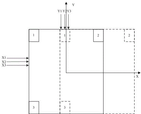
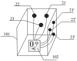
[0020] Such as figure 2 As shown, the calibration device consists of a detection frame 1, three X-direction photoelectric sensors 21,22,23, and three Y-direction photoelectric sensors 21', 22', 23'. Among them, the detection frame 1 is a square empty box, and its inner two adjacent surfaces are composed of 6 circular holes, respectively, each group of 3 circular holes is characterized in that the relative positional relationship of the 3 circular holes and the X-direction The layout of the measuring optical axis of the interferometer is consistent, and the relative position relationship between the three circular holes is consistent with the layout of the measuring optical axis of the Y-direction interferometer; the three X-direction photoelectric sensors 21, 22, 23 are installed on three In the three circular holes, three X-direction photoe...


PUM


Abstract

The invention discloses an interferometer error calibrating device for calibrating position errors of an interferometer. The interferometer error calibrating device comprises an X-direction photoelectric sensor, a Y-direction photoelectric sensor and a photoelectric sensor processing circuit. The X-direction photoelectric sensor comprises at least one photoelectric sensor located on one plane, and the Y-direction photoelectric sensor comprises at least one photoelectric sensor located on the other plane. The plane where the X-direction photoelectric sensor is located is perpendicular to the plane where the Y-direction photoelectric sensor is located. The photoelectric sensor processing circuit is used for converting photoelectric signals detected by the X-direction photoelectric sensor and the Y-direction photoelectric sensor into position information, and calculating the position errors of the interferometer according to the position information. The invention meanwhile discloses an interferometer error calibrating method.

Description

technical field [0001] The invention relates to the field of integrated circuit equipment manufacturing, in particular to an interferometer error calibration device and calibration method. Background technique [0002] In lithography equipment, the positioning accuracy of the moving stage not only affects the accuracy of the exposure position during the exposure process, but also affects the repeatability of the alignment system. Since the position measurement of the moving table usually uses a laser interferometer, and for the laser interferometer measurement system, the laser is greatly affected by the environment such as temperature and pressure. The direction of propagation will then change, resulting in a measurement error in position. Especially when the stroke of the test bench is large, it is difficult for the ambient air bath to control the temperature and pressure in the whole stroke, and as the distance between the two measuring axes of the interferometer increas...

Claims


Application Information

Patent Timeline
Patent Type & Authority Applications(China)
IPC IPC(8): G03F7/20
Inventor 徐伟
Owner SHANGHAI MICRO ELECTRONICS EQUIP (GRP) CO LTD
Why Eureka
Try Eureka