How to fix graphics

A pattern and to-be-repaired technology, which is applied in the field of correction of the key dimensions of the mask pattern and the field of correction patterns, can solve the problems such as the inability to guarantee that the key dimensions of the mask can meet the predetermined value range, the success rate is low, and the scrapping and so on.

Active Publication Date: 2019-03-29
SEMICON MFG INT (SHANGHAI) CORP
View PDF3 Cites 0 Cited by
  • Summary
  • Abstract
  • Description
  • Claims
  • Application Information

AI Technical Summary

Problems solved by technology

[0007] Under the existing technology, the critical dimension 130 of the finally formed mask pattern does not meet the predetermined size range, which leads to the need to scrap the mask, and according to the difference between the actual pattern size of the mask and the predetermined value range Correct the geometric data standard source data, exposure energy, development or etching time, the specific correction amount is determined according to the difference, and then use a new mask substrate to make again
However, this method not only cannot guarantee that the key dimensions of the remade mask after correction can meet the predetermined value range, but also causes waste of mask manufacturing costs.
[0008] In view of the above problems, there are other rework methods, such as coating the mask with a critical dimension that does not meet the predetermined value range with a photoresist layer, using the graphic data converted from the geometric data standard source data to align and expose the mask, and then Through a series of photolithography and etching processes to obtain a mask that meets the predetermined size range, but the success rate of doing so is extremely low
In the normal process flow, alignment is required before exposure, but in the rework process, it is difficult to completely align the pattern to be exposed with the pattern originally formed on the mask plate, which has limitations

Method used


Image

  • How to fix graphics
  • How to fix graphics
  • How to fix graphics

Examples


Embodiment Construction

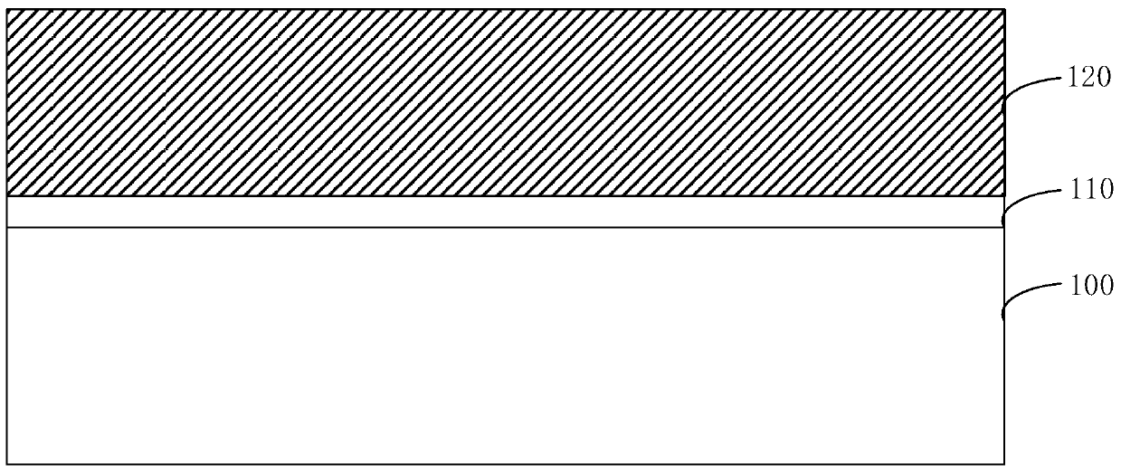
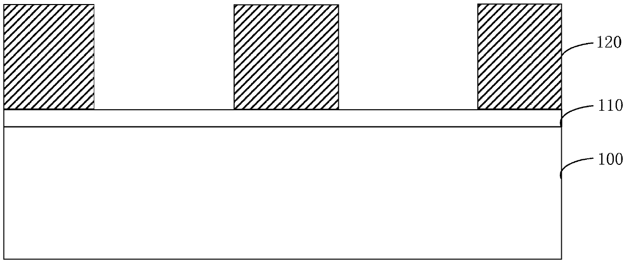
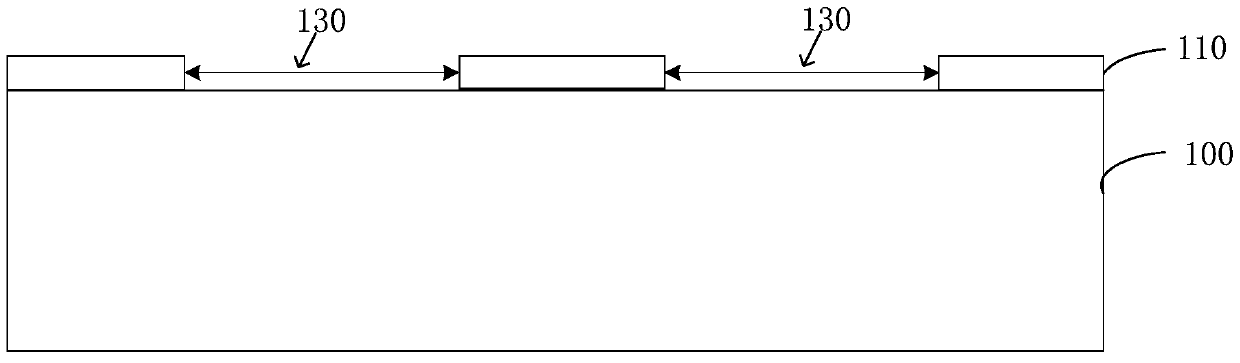
[0036] It can be seen from the background art that, in the process of manufacturing the mask, if the critical dimension of the pattern does not meet the predetermined value range, the mask will generally be reworked. Coating a photoresist layer on the mask plate to be reworked, and then through the processes of alignment, exposure, development, etching, and glue removal, a pattern that meets the predetermined value range of critical dimensions is obtained. However, due to the existing exposure technology, it is impossible to completely align the pattern to be etched with the pattern previously formed on the mask plate, so the success rate of rework is extremely low.

[0037] In order to solve the problem of low success rate of rework caused by low alignment accuracy, the inventors of the present invention conducted further research on the exposure process, and found that the graphic data converted from the standard source data of geometric data is not needed, and the exposure b...


PUM

PropertyMeasurementUnit
wavelengthaaaaaaaaaa

Abstract

A graph correction method includes the steps that when the size of a mask plate graph is smaller than a preset value range, and exposure light beams are emitted into the back side of a glass substrate by means of light transmittance of the glass substrate of a mask plate and light tightness of a shading layer and emitted into a photoresist layer from the shading layer for exposure of the photoresist layer; a to-be-etched pattern is formed after development; the photoresist layer is left after etching and development, so the critical size of the to-be-etched pattern is increased to the preset value range; the etched photoresist layer serves as a mask, the to-be-etched pattern with the critical size increased etches the shading layer till the glass substrate is exposed, and the pattern in the preset size range is formed. By means of the method, during exposure, alignment is not needed, and accordingly the problem that alignment precision is low during exposure is solved.

Description

technical field [0001] The invention relates to the field of semiconductor manufacturing, in particular to a method for correcting patterns, especially the correction of key dimensions of mask pattern. Background technique [0002] With the continuous development of ultra-large integrated circuits, the circuit design becomes more and more complex, the feature size becomes smaller and smaller, and the impact of the feature size of the circuit on the performance of the device is also increasing. The mask is an important medium for transferring the circuit pattern to the silicon wafer, and the critical size of the mask pattern directly affects the actual pattern size on the silicon wafer, and ultimately affects the yield of the product. With the continuous development of technology, the critical dimension of the mask pattern is on the order of microns, so the requirements for the critical dimension of the mask pattern are getting higher and higher. To ensure the accuracy of th...

Claims


Application Information

Patent Timeline
Patent Type & Authority Patents(China)
IPC IPC(8): G03F9/00
Inventor 张士健
Owner SEMICON MFG INT (SHANGHAI) CORP
Why Eureka
Try Eureka