Embedded transparent circuit board and manufacturing method thereof

A technology for transparent circuit boards and manufacturing methods, which is applied in multilayer circuit manufacturing, circuit substrate materials, printed circuit manufacturing, etc., and can solve the problems of low connection reliability of flexible copper clad substrates, unfavorable component inspection, easy shrinkage and wrinkles, etc. , to achieve the effect of testing and improving the reliability of the connection

Active Publication Date: 2022-06-24
AVARY HLDG (SHENZHEN) CO LTD +1
View PDF7 Cites 0 Cited by
  • Summary
  • Abstract
  • Description
  • Claims
  • Application Information

AI Technical Summary

Problems solved by technology

Therefore, when printing solder paste to mount electronic components, PET and PEN are very easy to shrink and wrinkle, resulting in low reliability of the connection between electronic components and the flexible copper clad substrate
If non-light-transmitting materials are used, there will be a problem of low alignment accuracy, which is not conducive to component inspection

Method used


Image

  • Embedded transparent circuit board and manufacturing method thereof
  • Embedded transparent circuit board and manufacturing method thereof
  • Embedded transparent circuit board and manufacturing method thereof

Examples


Embodiment Construction

[0049] In order to further illustrate the technical means and effects adopted by the present invention to achieve the predetermined purpose of the invention, the following are combined with the following annexes. Figure 1-6 And the preferred embodiment, the specific embodiment, structure, feature and effect of the manufacturing method of the embedded transparent circuit board provided by the present invention are described in detail as follows.

[0050] see Figure 1-6 , the present invention provides a manufacturing method of the embedded transparent circuit board 100, including the following steps:

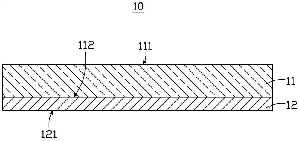
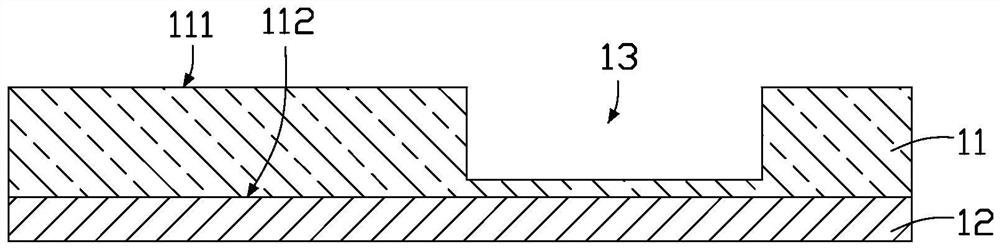
[0051] As a first step, see figure 1 , to provide a first copper clad substrate 10 , the first copper clad substrate 10 includes a first transparent dielectric layer 11 and a first copper foil layer 12 formed on the first transparent dielectric layer 11 .

[0052] The first transparent medium layer 11 includes a first surface 111 and a second surface 112 opposite to the first...


PUM


Abstract

An embedded transparent circuit board, comprising: a first circuit substrate, including a first transparent medium layer and a first conductive circuit layer formed on the first transparent medium layer; grooves are formed on the first transparent medium layer, at least one The electronic components are accommodated and fixed in the groove; the second circuit substrate includes the second transparent medium layer and the second conductive circuit layer formed on the second transparent medium layer; the surface of the first conductive circuit layer and the second conductive circuit layer and a blackening layer is formed on the side; and transparent glue, the first transparent medium layer, transparent glue and the second transparent medium layer are stacked together in sequence; the transparent glue is filled in the gap between the inner wall of the groove and the electronic component, The first conductive circuit layer or the second conductive circuit layer is electrically connected to the electronic components. The invention also provides a method for manufacturing the embedded transparent circuit board. The embedded transparent circuit board provided by the invention has better connection reliability.

Description

technical field [0001] The invention relates to a printed circuit board technology, in particular to an embedded transparent circuit board and a manufacturing method thereof. Background technique [0002] With the continuous development of electronic products in the direction of light weight, high frequency, high density and high performance, and in some specific scenarios, transparent electronic products gradually show their various advantages. In order to realize the transparency of electronic products, there is an increasing demand for transparent printed circuit boards, such as mice, earphones, antennas, etc. [0003] At present, transparent media such as polyethylene terephthalate (PET) and polyethylene naphthalate (polyethylene naphthalate two formic acid glycol ester, PEN) are widely used in the industry to form flexible copper clad laminates to make transparent flexible laminates. circuit board. PET and PEN have the problem of insufficient heat resistance, which ma...

Claims


Application Information

Patent Timeline
Patent Type & Authority Patents(China)
IPC IPC(8): H05K1/03H05K1/18H05K3/46
CPCH05K1/185H05K1/03H05K3/4611H05K3/4697
Inventor 李艳禄沈芾云
Owner AVARY HLDG (SHENZHEN) CO LTD
Why Eureka
Try Eureka