NAND FLASH testing method

A test method and bad block table technology, applied in the field of NANDFLASH testing, can solve problems such as incomplete original bad block table information, unstable blocks cannot be found, digital product data errors, etc., so as to improve the test accuracy and reduce the repair rate. and defect rate, the effect of ensuring the correctness of the data

Inactive Publication Date: 2016-11-23
BIWIN STORAGE TECH CO LTD
View PDF7 Cites 16 Cited by
  • Summary
  • Abstract
  • Description
  • Claims
  • Application Information

AI Technical Summary

Problems solved by technology

[0003] The existing NAND FLASH will have initial factory information when it leaves the factory. Digital solution providers can use this information to create the original bad block table, but the information in the original bad block table may not be comprehensive enough, especially in some special cases, such as high temperature. Unstable blocks cannot be found, causing data errors in digital products at high temperatures and system crashes

Method used


Image

  • NAND FLASH testing method
  • NAND FLASH testing method
  • NAND FLASH testing method

Examples


Embodiment 1

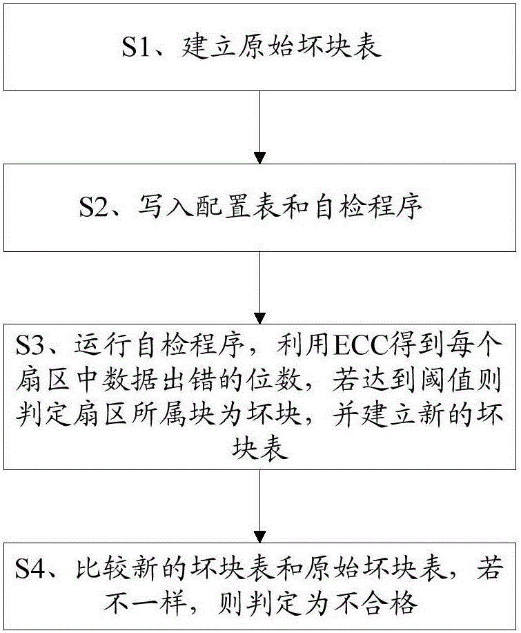
[0041] Please refer to figure 1 , Embodiment one of the present invention is: a kind of NAND FLASH test method, specifically comprises the following steps:

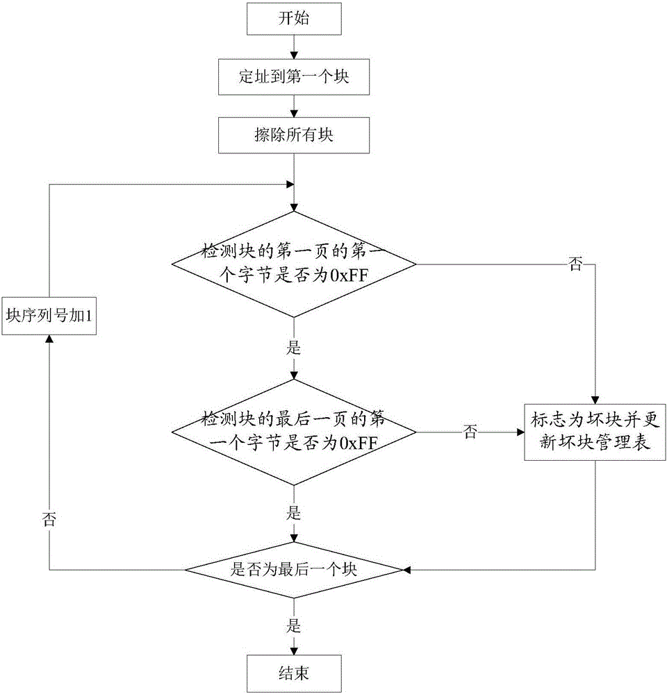
[0042] S1. Establish an original bad block table. Specifically, check whether the first byte of the first page and the last page of each block are both 0xFF, if so, it is a good block, otherwise it is a bad block. Such as figure 2 Shown is the specific flowchart of establishing the original bad block table, which may specifically include the following steps:

[0043] S11, addressing to the first block, erasing all physical blocks of NAND FLASH;

[0044] S12, whether the first byte of the first page of the detection block is 0xFF, if so, enter step S13, otherwise enter step S14;

[0045] S13, whether the first byte of the last page of detection block is 0xFF, if then enter step S15, if otherwise enter step S14;

[0046] S14, mark as a bad block and update the bad block management table, and enter step S15;
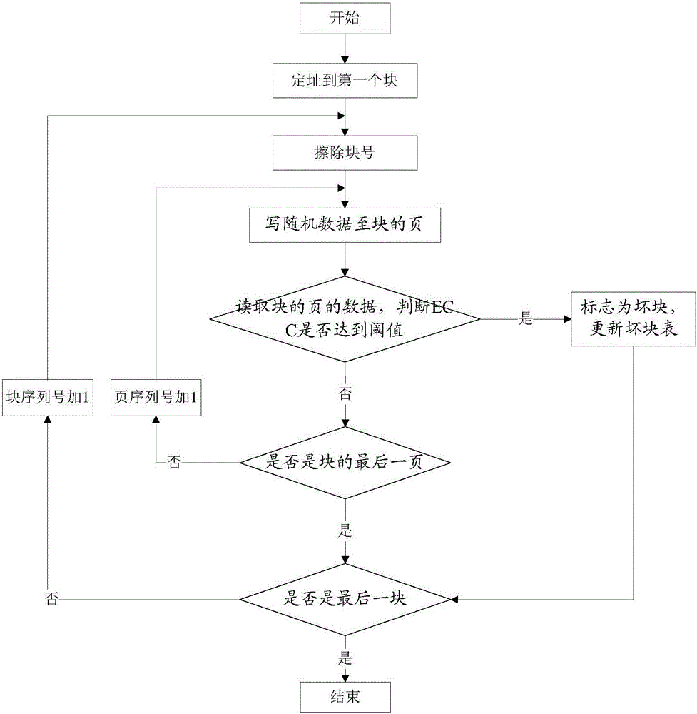
[0047] ...


PUM


Abstract

The invention discloses a NAND FLASH testing method, comprising the following steps: S1, establishing an original bad block table; S2, writing a configuration table and a self-inspection program; S3, running the self-inspection program, and using ECC to obtain data in each sector If the number of wrong bits reaches the threshold, it is determined that the block to which the sector belongs is a bad block, and a new bad block table is established; S4, if the newer bad block table and the original bad block table are not the same, then it is judged as unqualified. The invention uses ECC to obtain a new bad block table, and compares it with the original bad block table to judge whether it is qualified, which can further improve the test accuracy, avoid putting data in an unstable storage space, and make digital devices more stable in use and longer in service life. longer.

Description

technical field [0001] The invention relates to the field of NAND FLASH, in particular to a NAND FLASH testing method. Background technique [0002] If digital products need to use storage devices, they have the opportunity to use NAND FLASH. NAND FLASH is composed of one or more NAND granules, and each granule contains many blocks, a block is the unit of NAND FLASH erasing; and a block contains multiple pages, and a page is the smallest unit of programming; The page contains multiple sectors, and the unit of ecc (error detection and correction) is sector, and the reported ecc number is based on how many bits are wrong in the sector. In the case of more and more digital products, the stability and security of storage devices ensure the correctness of digital product data and the stability of the system. Therefore, to find out the unstable factors of the nand flash storage device, that is, to find out the relatively fragile blocks and unstable blocks in the blocks composed ...

Claims


Application Information

Patent Timeline
Patent Type & Authority Applications(China)
IPC IPC(8): G11C29/42
CPCG11C29/42
Inventor 孙日欣孙成思李振华黄善勇叶欣张翔邝祖智
Owner BIWIN STORAGE TECH CO LTD
Why Eureka
Try Eureka