
Flash memory and forming method thereof

A technology of flash memory and storage unit, which is applied in the field of flash memory, can solve problems such as insulation layer peeling, and achieve the effect of avoiding peeling off

Active Publication Date: 2016-11-30
SHANGHAI HUAHONG GRACE SEMICON MFG CORP
View PDF3 Cites 2 Cited by
  • Summary
  • Abstract
  • Description
  • Claims
  • Application Information

AI Technical Summary

Problems solved by technology

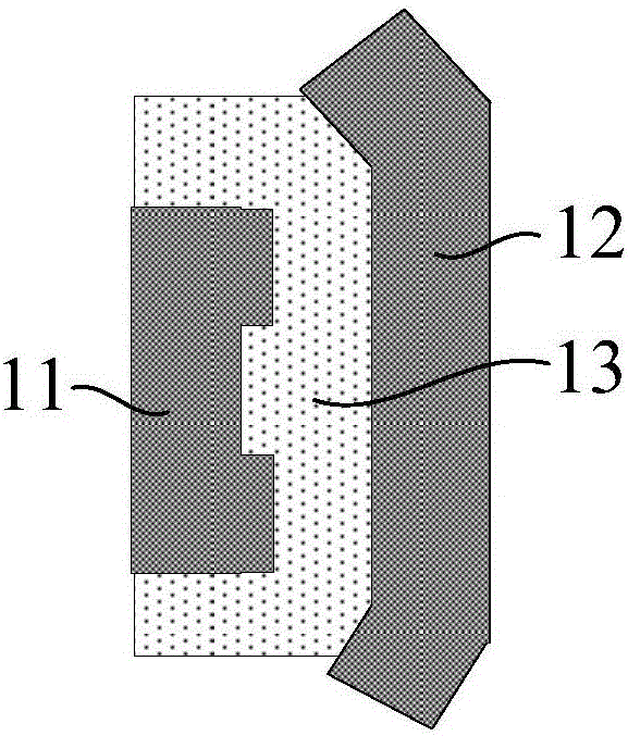
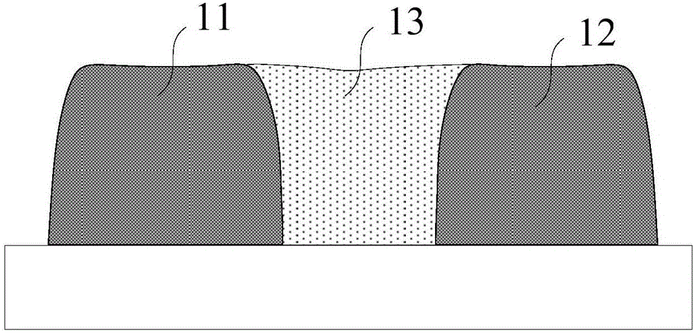
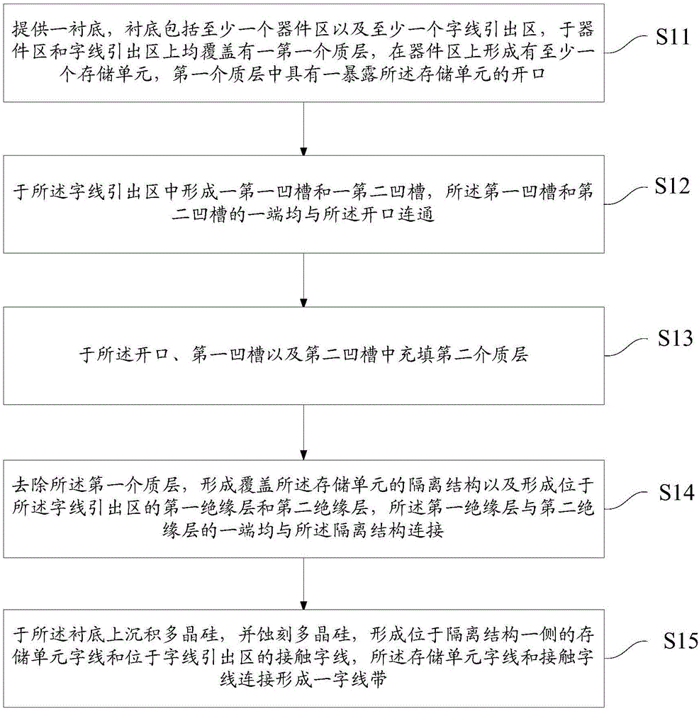
[0005] The object of the present invention is to provide a flash memory and a method for forming the flash memory, so as to solve the problem that the insulating layer used to support the contact word line is prone to peeling off in the existing flash memory

Method used


Image

  • Flash memory and forming method thereof
  • Flash memory and forming method thereof
  • Flash memory and forming method thereof

Examples


Embodiment Construction

[0042]As mentioned in the background, word lines of memory cells for controlling erasing and programming are formed in the flash memory, so that the problem of over-erasing can be avoided. When forming a contact word line in the word line lead-out region to lead out a memory cell word line located on one side of the memory cell, the contact word line is usually formed between two insulating layers, that is, through the two insulating layers. support, so that the subsequently formed contact word line has a certain height and surface flatness, thereby ensuring that the signal transmission between the conductive plug formed on the contact word line and the contact word line is normal. However, among the two insulating layers used to support the contact word line, one of the insulating layers is usually an isolated structure, and the contact area between the isolated structure and the substrate is small, so when forming the insulating layer, The isolated insulating layer is very e...


PUM


Abstract

The invention provides a flash memory and a forming method thereof. The flash memory comprises at least one device area and at least one word line lead-out area, wherein the device area is provided with an isolation structure of an isolating memory unit; the word line lead-out area is provided with a first insulating layer and a second insulating layer; and one end of each of the first insulating layer and the second insulating layer is connected to the isolation structure, so that an independent island structure of the first insulating layer and the second insulating layer can be avoided; and the phenomenon that the first insulating layer is separated from the second insulating layer can be effectively avoided in the forming process of the flash memory.

Description

technical field [0001] The invention relates to the technical field of semiconductors, in particular to a flash memory and a method for forming the flash memory. Background technique [0002] Flash memory (Flash EPROM) is a form of electronically erasable programmable read-only memory (electrically erasable programmable read-only memory EEPROM). Flash memory is widely used in portable computers, mobile phones, In electronic products such as digital music players. Flash memory is a kind of non-volatile memory. Its operating principle is to control the switch of the gate channel by changing the critical voltage of the storage unit, so as to achieve the purpose of storing data, so that the data stored in the storage unit will not be lost due to power interruption. disappear. [0003] According to the different gate structures of the transistors constituting the memory cells, generally, flash memory can be divided into two types: stacked gate flash memory and split gate flash...

Claims


Application Information

Patent Timeline
Patent Type & Authority Applications(China)
IPC IPC(8): H01L27/115H01L21/8247H01L21/8239H01L21/8234H01L21/311H10B41/35H10B69/00H10B99/00
CPCH01L21/311H01L21/8234H10B99/00H10B69/00
Inventor 王卉曹子贵陈宏徐涛
Owner SHANGHAI HUAHONG GRACE SEMICON MFG CORP
Learn More