A magnetic stress-relieving mounting method for thin planar optical elements

An optical element and stress relief technology, which is applied in the field of the upper plate of the element, can solve the problems of the large surface change of the thin plane element, the difficulty in controlling the height of the adhesive layer, and the technical dependence of the processing personnel. , easy to operate, easy to control the effect

Active Publication Date: 2018-08-14
SHANGHAI INST OF OPTICS & FINE MECHANICS CHINESE ACAD OF SCI
View PDF8 Cites 0 Cited by
  • Summary
  • Abstract
  • Description
  • Claims
  • Application Information

AI Technical Summary

Problems solved by technology

However, the adhesive glue (such as asphalt) on the traditional dispensing plate has different melting speeds on the bonding plate, and the size of the asphalt glue point is uneven, which requires the processing personnel to have better technical requirements. Therefore, the traditional plate-on-plate mode often appears as follows Problems: poor parallelism of planar components, difficulty in controlling the height of the adhesive layer, and great dependence on the technology of processing personnel; especially the shape of the upper and lower discs of thin planar components changes greatly
Generally speaking, the overall effect of dispensing glue on the plate is relatively poor

Method used


Image

  • A magnetic stress-relieving mounting method for thin planar optical elements
  • A magnetic stress-relieving mounting method for thin planar optical elements

Examples


Embodiment Construction

[0025] The present invention will be further described below in conjunction with the accompanying drawings, but the protection scope of the present invention should not be limited thereby.

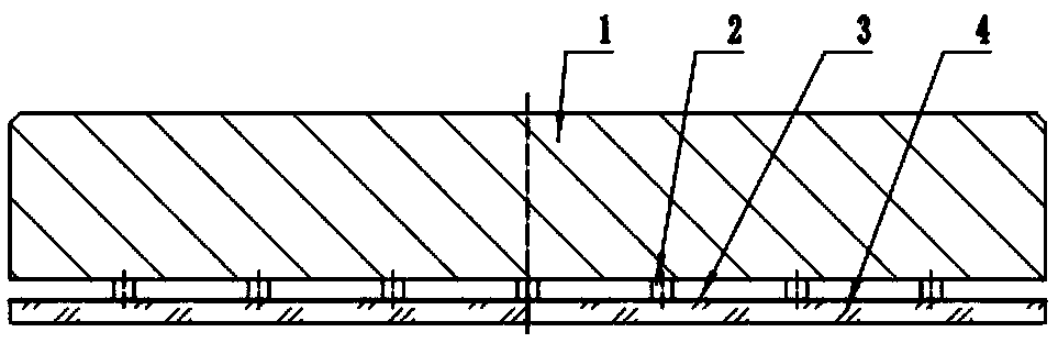
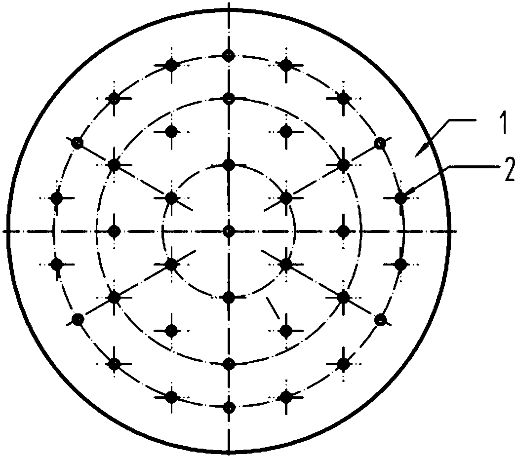
[0026] see first figure 1 , figure 1 It is a rear side view of the magnetic stress-relief optical element of the present invention, and it can be seen from the figure that after the optical element is mounted, it includes an upper plate substrate 1, a magnet block 2, an adhesive film (double-sided adhesive tape) 3 and a thin film from top to bottom. Shaped planar optical element 4.

[0027] The specific processing procedures are as follows:

[0028] Firstly, cover a layer of adhesive film 3 on the surface of the upper plate of the thin planar optical element 4 to be processed, magnetize the processed cylindrical magnet block 2, and place it on the upper plate substrate 1 according to the designed arrangement Paste the cylindrical magnet block 2, put the side of the thin planar optical e...


PUM


Abstract

The invention discloses a magnetic stress relief bonding pad loading method for thin planar optical elements, comprising 1) processing cylindrical magnet blocks with the diameters of 2-10mm and the thicknesses of 2-5mm; 2) magnetizing the processed cylindrical magnet blocks; 3) reducing the planeness errors of working surfaces of bonding pad loading substrates to be smaller than 0.01mm by using a grinding method; 4) placing the cylindrical magnet blocks on the working surfaces of the bonding pad loading substrates according to a designed arrangement way; and 5) cleaning to-be-processed elements, pasting a layer of binding film (a double-sided adhesive tape) on each bonding pad loading surface, and then, vertically applying a pressure to enable the to-be-processed elements to be in complete contact with the cylindrical magnet blocks among the bonding pad loading substrates. The method disclosed by the invention is simple in process, easy to operate and capable of keeping the operating environment clean and pollution-free; and the surface shapes of the elements subjected to bonding pad loading by using the method can be kept unchanged after the elements are processed and taken down, so that the magnetic stress relief bonding pad loading method is suitable for batch production of high-precision thin planar elements.

Description

technical field [0001] The invention relates to the technical field of component loading in optical cold working technology, in particular to a method for magnetic stress-relieving loading of thin planar components. Background technique [0002] Planar optical components whose diameter (or side length) to thickness ratio is greater than 15:1 are generally called thin planar components in optics. During processing, components usually appear due to bonding tension, temperature changes and other external forces. The surface deformation cannot meet the designed surface accuracy requirements, especially the larger the diameter to thickness ratio, the greater the deformation of components with high surface accuracy and parallelism requirements, and the greater the processing difficulty. The ratio of the diameter to the thickness of the component is 27:1, which is defined as an "ultra-thin" component. Due to its small thickness, the thin planar component has poor rigidity and is ea...

Claims


Application Information

Patent Timeline
Patent Type & Authority Patents(China)
IPC IPC(8): B24B13/005B24B13/00
CPCB24B13/0018B24B13/0052
Inventor 高文兰朱宝玪徐学科顿爱欢吴福林邵建达
Owner SHANGHAI INST OF OPTICS & FINE MECHANICS CHINESE ACAD OF SCI
Why Eureka
Try Eureka