
A kind of array substrate and display device

An array substrate, electrostatic protection technology, applied in instruments, nonlinear optics, optics, etc., can solve problems such as electrostatic breakdown of data lines and inability to achieve basic functions

Active Publication Date: 2020-06-02
BOE TECH GRP CO LTD
View PDF11 Cites 0 Cited by
  • Summary
  • Abstract
  • Description
  • Claims
  • Application Information

AI Technical Summary

Problems solved by technology

[0005] In the existing display manufacturing process, the inventors found that during the manufacturing process of the product, the functional wires in the wiring-intensive area, such as gate lines and data lines, are prone to electrostatic breakdown, and the electrostatic discharge is carried out by conducting them with the electrostatic circuit The static electricity accumulated on these functional wires can be discharged, but if the gate wire or data wire is directly connected to the static wire, it will not be able to realize the basic function

Method used


Image

  • A kind of array substrate and display device
  • A kind of array substrate and display device
  • A kind of array substrate and display device

Examples


Embodiment Construction

[0068] The technical solutions in the embodiments of the present invention will be clearly and completely described below in conjunction with the accompanying drawings in the embodiments of the present invention. Obviously, the described embodiments are only a part of the embodiments of the present invention, rather than all the embodiments. Based on the embodiments of the present invention, all other embodiments obtained by those of ordinary skill in the art without creative work shall fall within the protection scope of the present invention.

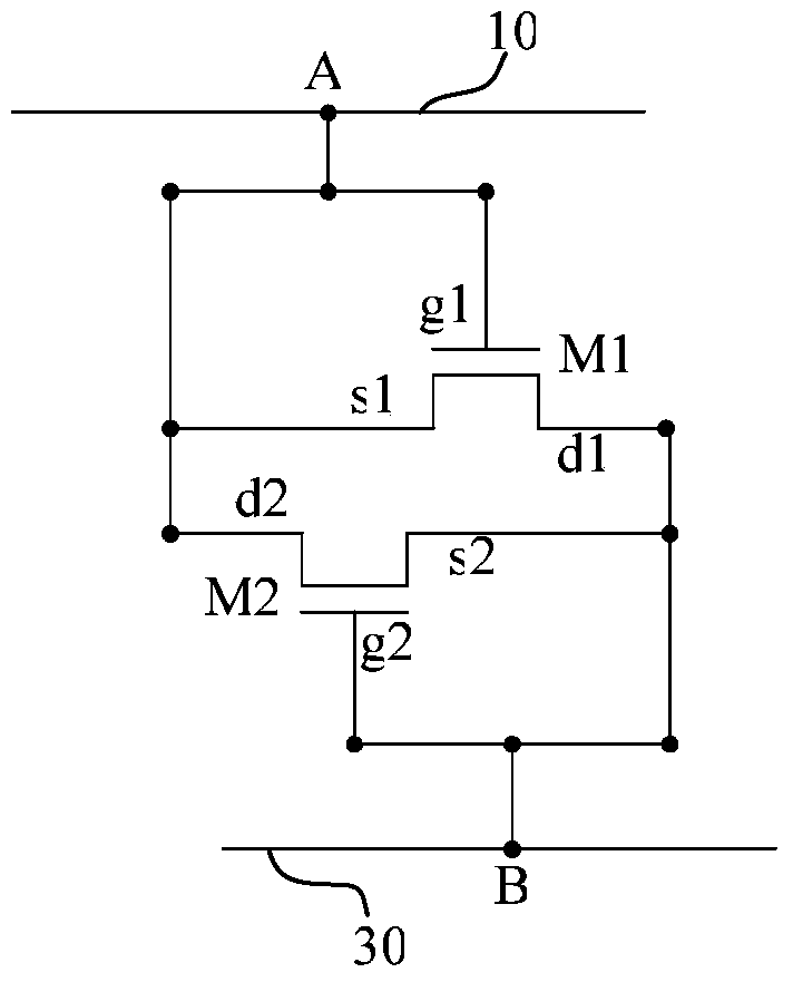
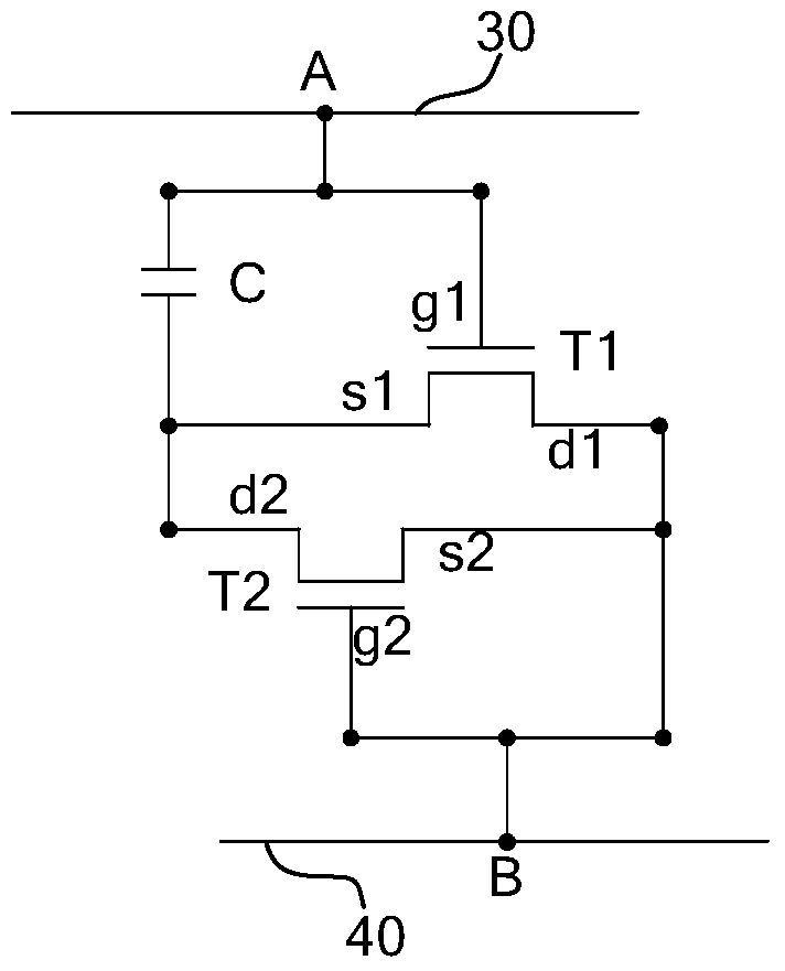
[0069] The transistors used in all the embodiments of the present invention can be thin film transistors or field effect transistors or other devices with the same characteristics. In addition, in the following schemes, g represents the gate of the transistor, s represents the source of the transistor, and d represents the drain of the transistor.

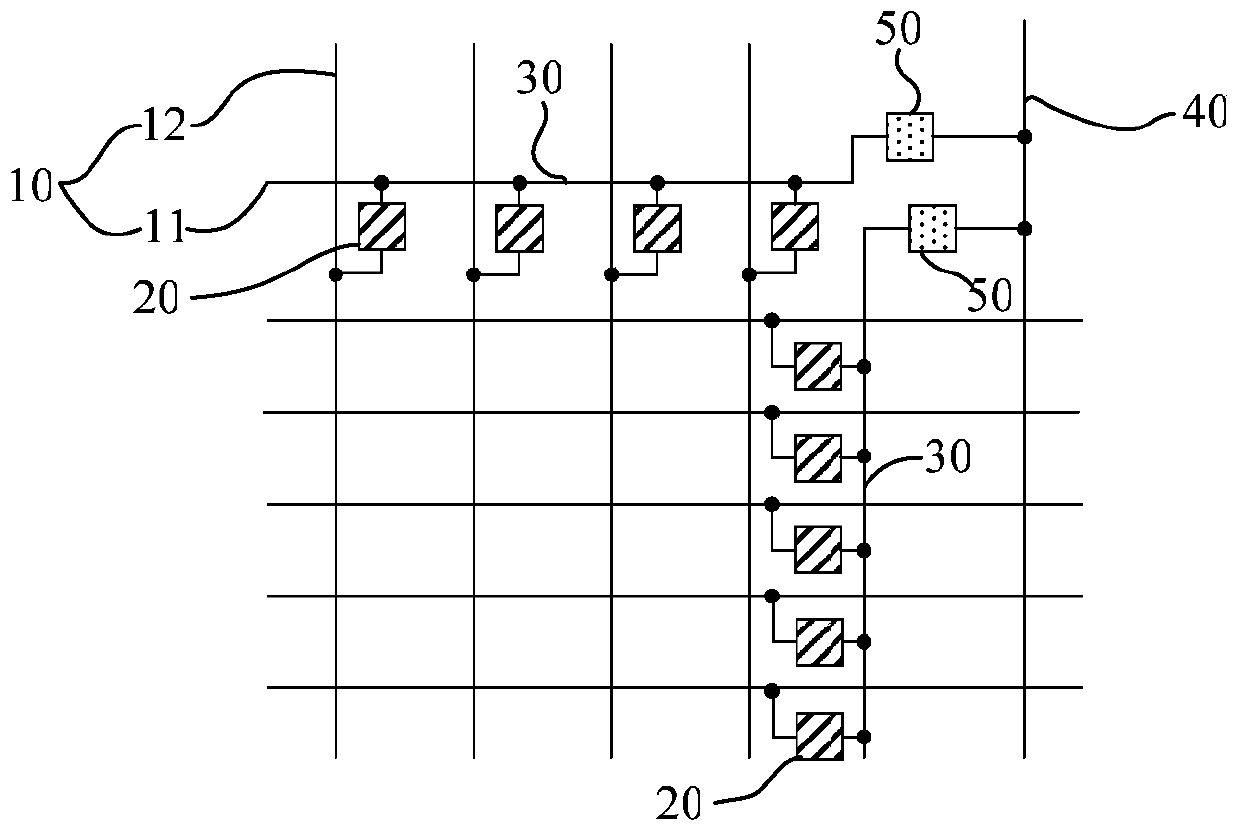
[0070] Reference figure 1 As shown, the embodiment of the present invention provides an arr...


PUM


Abstract

The embodiment of the invention provides an array substrate and a display device, and relates to the technical field of display. A functional wire in a product can be effectively subjected to static release, and implementation of the normal function of the product is not influenced. The array substrate is characterized by comprising a signal input lead, a first static protection unit, a second static protection unit, a static protection wire and a common electrode wire; the signal input lead is connected to the static protection wire through the first static protection unit; the static protection wire is connected to the common electrode wire through the second static protection unit; the second static protection unit is used for isolating direct-current components on the static protection wire or the common electrode wire; when static occurs, the static is released from the static protection wire to the common electrode wire through the second static protection wire, or the static is released from the common electrode wire to the static protection wire through the second static protection unit.

Description

Technical field [0001] The embodiments of the present invention relate to the field of display technology, and in particular, to an array substrate and a display device. Background technique [0002] Liquid crystal display technology is widely used in TVs, mobile phones and public information displays. Liquid crystal displays may be damaged by static electricity during the manufacturing process or in use. [0003] The accumulation and release of static electricity is one of the main factors causing device damage in the semiconductor field. The function of ESD (Electro-Static Discharge) protection circuit is to effectively block or drain static electricity and prevent devices from being damaged by static electricity. Whether it can better block or drain static electricity, the key is the rationality of the ESD design. [0004] ESD breakdown voltage V B ∝E B d, E in the formula B Is the critical electric field for the breakdown of the insulating layer, which is related to the materia...

Claims


Application Information

Patent Timeline
Patent Type & Authority Patents(China)
IPC IPC(8): G02F1/1362
CPCG02F1/136204G02F1/136286
Inventor 程鸿飞
Owner BOE TECH GRP CO LTD
Learn More