Forming method of semiconductor structure

A semiconductor and structural part technology, applied in the field of semiconductor structure formation, can solve the problems of dummy gate structure damage, affecting the performance of semiconductor structures, etc.

Active Publication Date: 2016-12-07
SEMICON MFG INT (SHANGHAI) CORP
View PDF3 Cites 5 Cited by
  • Summary
  • Abstract
  • Description
  • Claims
  • Application Information

AI Technical Summary

Problems solved by technology

[0006] In the prior art, in the process of etching the fins on both sides of the dummy gate structure, the dummy gate structure is often damaged, which affects the performance of the formed semiconductor structure.

Method used


Image

  • Forming method of semiconductor structure
  • Forming method of semiconductor structure
  • Forming method of semiconductor structure

Examples


Embodiment Construction

[0034] As mentioned in the background art, the performance of the semiconductor structure formed in the prior art needs to be further improved.

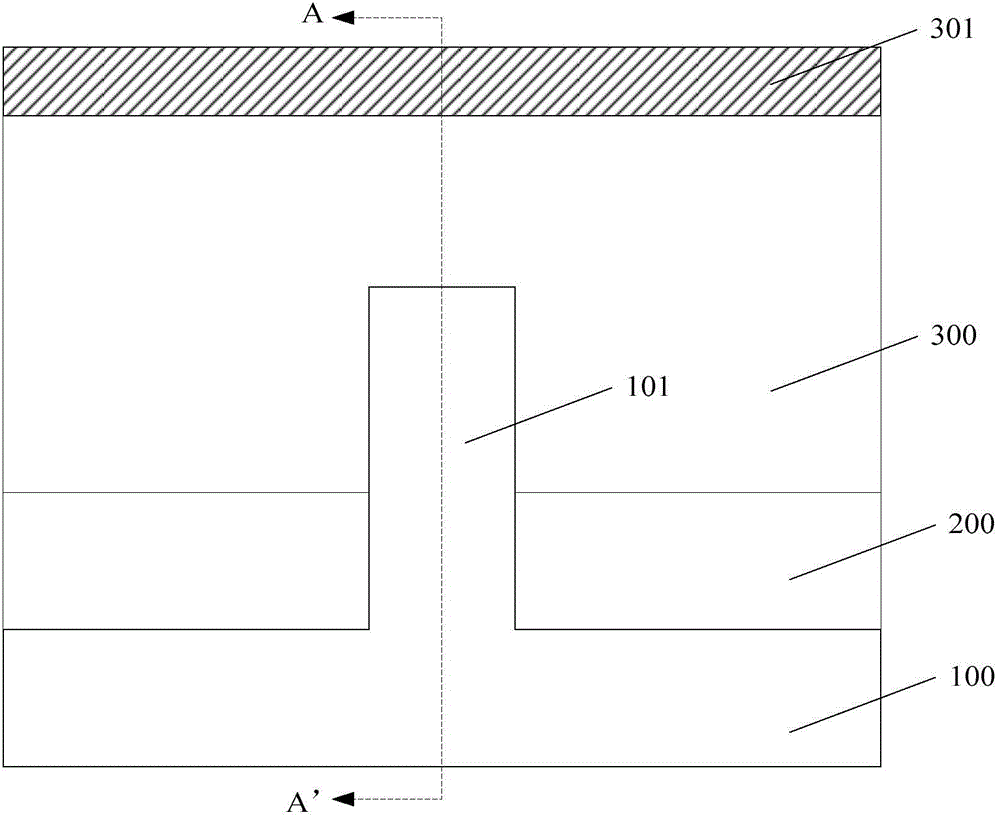
[0035] Research has found that after the formation of the dummy gate structure, sidewalls are usually formed on the surface of the side walls of the dummy gate structure, and a mask layer is provided on the top of the dummy gate structure to protect the surface of the dummy gate structure. In the process of etching the fins on both sides of the dummy gate structure to form grooves, the sidewalls on both sides of the dummy gate structure and the mask layer on the top of the dummy gate structure are often damaged, resulting in the exposure of the surface of the dummy gate structure. When the stress material is filled in the groove subsequently, the stress material will also be formed when the dummy gate structure appears, and the dummy gate structure will be removed later to form the gate structure, which will cause an electrical gap be...


PUM


Abstract

The invention provides a forming method of a semiconductor structure. The method comprises the steps that a semiconductor substrate is provided; a fin is formed on the surface of the semiconductor substrate; an isolating layer is formed on the surface of the semiconductor substrate; the surface of the isolating layer is lower than the top surface of the fin and covers one part of side wall of the fin; a pseudo gate structure stretching across the fin is formed on the isolating layer and covers one part of side wall and the top part of the fin; a hard mask layer is arranged at the top part of the pseudo gate structure; side walls are formed on the side wall surfaces of the pseudo gate structure and the hard mask layer; the fin at two sides of the pseudo gate structure is etched to form grooves; a protective layer is formed on the surfaces of the grooves and the isolating layer; the surface of the protective layer is higher than the top surface of the fin to expose one part of pseudo gate structure; supplement side walls are formed on the side walls of the exposed pseudo gate structure; and the protective layer is removed. By the method, the performance of the formed semiconductor substrate can be improved

Description

technical field [0001] The invention relates to the technical field of semiconductors, in particular to a method for forming a semiconductor structure. Background technique [0002] With the continuous development of semiconductor process technology, process nodes are gradually reduced, and gate-last (gate-last) process has been widely used to obtain an ideal threshold voltage and improve device performance. However, when the feature size of the device is further reduced, even if the gate-last process is adopted, the structure of the conventional MOS field effect transistor can no longer meet the requirements for device performance, and the fin field effect transistor (Fin FET) is obtained as a multi-gate device. received widespread attention. [0003] At the same time, in order to further improve the performance of transistors, stress engineering is introduced into the transistor manufacturing process. Applying compressive stress to the channel region of the transistor ca...

Claims


Application Information

Patent Timeline
Patent Type & Authority Applications(China)
IPC IPC(8): H01L21/336
Inventor 张海洋肖芳元
Owner SEMICON MFG INT (SHANGHAI) CORP
Why Eureka
Try Eureka