
Printed circuit board and mobile terminal

A technology of printed circuit boards and electronic devices, which is applied in the field of communication, can solve problems affecting the welding stability and heat dissipation of QFN packaged devices, welding bubbles and cavities, and solder extension, so as to ensure the welding stability and heat dissipation. Effect

Inactive Publication Date: 2016-12-14
NUBIA TECHNOLOGY CO LTD
View PDF6 Cites 6 Cited by
  • Summary
  • Abstract
  • Description
  • Claims
  • Application Information

AI Technical Summary

Problems solved by technology

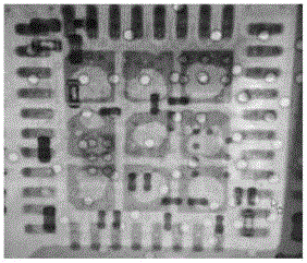
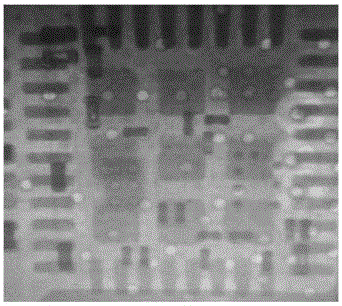
[0002] Existing mobile phone PCBs (ie: printed circuit boards) have devices with large pads (ie: electronic devices, such as QFN packaged devices), and due to performance such as heat dissipation, it is necessary to design a large ground pad (equivalent to the "main soldering pad" in this application). disc"), and the existing traditional soldering, the large ground pad (size 3mm*3mm) is directly soldered to the QFN packaged device, because the size of the large ground pad is large, the fluidity of the solder is poor during the high-temperature melting process of the reflow furnace, As a result, the solder cannot be extended on the surface of the large grounding pad, so that there will be no solder in some places on the large grounding pad, that is, welding bubbles and voids will be formed (can be detected by X-RAY detector), affecting QFN Soldering stability and heat dissipation of packaged devices

Method used


Image

  • Printed circuit board and mobile terminal
  • Printed circuit board and mobile terminal
  • Printed circuit board and mobile terminal

Examples


Embodiment Construction

[0027] It should be understood that the specific embodiments described here are only used to explain the present invention, not to limit the present invention.

[0028] A mobile terminal implementing various embodiments of the present invention will now be described with reference to the accompanying drawings. In the following description, use of suffixes such as 'module', 'part' or 'unit' for denoting elements is only for facilitating description of the present invention and has no specific meaning by itself. Therefore, "module" and "component" may be used mixedly.

[0029] Mobile terminals may be implemented in various forms. For example, terminals described in the present invention may include devices such as mobile phones, smart phones, notebook computers, digital broadcast receivers, PDAs (Personal Digital Assistants), PADs (Tablet Computers), PMPs (Portable Multimedia Players), navigation devices, etc. mobile terminals and fixed terminals such as digital TVs, desktop c...


PUM

PropertyMeasurementUnit
Sizeaaaaaaaaaa
Sizeaaaaaaaaaa
Sizeaaaaaaaaaa

Abstract

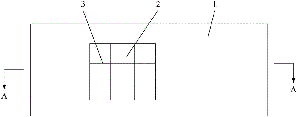
The invention discloses a printed circuit board and a mobile terminal. The printed circuit board comprises a board body having a first region for main welding plate arrangement, a main welding plate arranged at the first region, solder separation bars, soldering tin layers, and an electronic device. The solder separation bars arranged at the first region divide the main welding plate into a plurality of sub welding plates and are used for preventing the series flowing of soldering tin among the adjacent sub welding plates during the welding process. The soldering tin layers are arranged on the sub welding plates. The electronic device arranged at the first region is connected with the sub welding plates by the soldering tin layer. According to the provided printed circuit board, because the main welding plate are divided into multiple sub welding plates by the solder separation bars and the dimensions of the sub welding plates are smaller than that of the main welding plate, the soldering tin can be arranged on all sub welding plates during the welding process and welding bubbles and holes in the soldering tin layers are prevented, thereby guaranteeing stability and the heat radiation performance of the QFN packaging device welding.

Description

technical field [0001] The invention relates to communication technology, in particular to a printed circuit board and a mobile terminal. Background technique [0002] Existing mobile phone PCBs (ie: printed circuit boards) have devices with large pads (ie: electronic devices, such as QFN packaged devices), and due to performance such as heat dissipation, it is necessary to design a large ground pad (equivalent to the "main soldering pad" in this application). disc"), and the existing traditional soldering, the large ground pad (size 3mm*3mm) is directly soldered to the QFN packaged device, because the size of the large ground pad is large, the fluidity of the solder is poor during the high-temperature melting process of the reflow furnace, As a result, the solder cannot be extended on the surface of the large grounding pad, so that there will be no solder in some places on the large grounding pad, that is, welding bubbles and voids will be formed (can be detected by X-RAY d...

Claims


Application Information

Patent Timeline
IPC IPC(8): H05K1/11
CPCH05K1/111H05K2201/09372
Inventor 刘文武
Owner NUBIA TECHNOLOGY CO LTD
Learn More