Supercharge Your Innovation With Domain-Expert AI Agents!

Saw device manufacturing method

A manufacturing method and device technology, which is applied in the direction of manufacturing tools, semiconductor devices, electrical components, etc., can solve the problems of easy degradation of SAW device quality and achieve the effect of suppressing quality degradation

Inactive Publication Date: 2017-01-04
DISCO CORP
View PDF10 Cites 1 Cited by
  • Summary
  • Abstract
  • Description
  • Claims
  • Application Information

AI Technical Summary

Problems solved by technology

[0006] However, if the SAW device wafer including the clad layer made of resin is cut and divided with a cutting tool, cracks (flaking) will occur in the clad layer and the quality of the SAW device will easily deteriorate.

Method used


Image

  • Saw device manufacturing method
  • Saw device manufacturing method
  • Saw device manufacturing method

Examples


Embodiment Construction

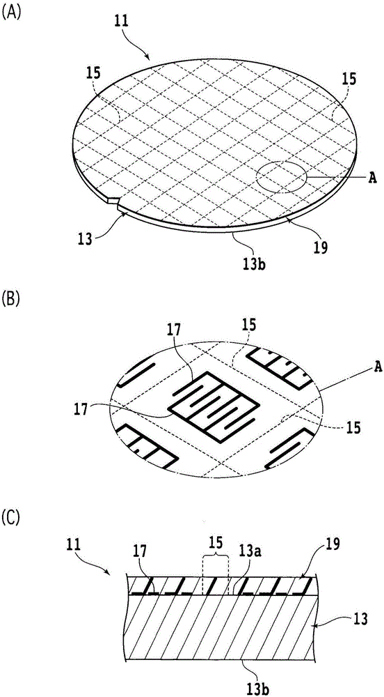
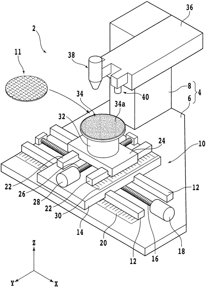
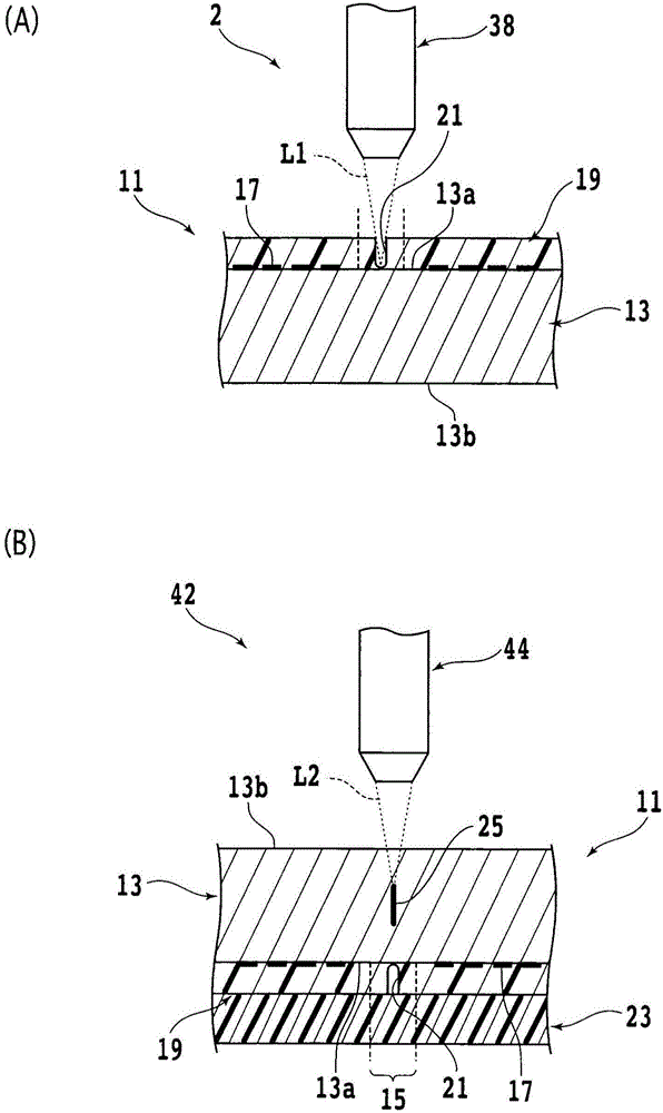
[0020] Embodiments of the present invention will be described with reference to the drawings. The manufacturing method of the SAW (Surface Acoustic Wave: Surface Acoustic Wave) device of the present embodiment includes a laser machining groove forming step (refer to image 3 (A)), modified layer formation process (refer to image 3 (B)) and the division process (refer to Figure 4 ). In the laser machining groove forming step, laser beams are irradiated to the clad layer constituting the SAW device wafer to form laser machining grooves along planned division lines (streets).

[0021] In the modified layer forming step, the crystallized substrate constituting the SAW device wafer is irradiated with laser light to form modified layers along the planned division lines. In the dividing step, an external force is applied to the SAW device wafer to divide the SAW device wafer into a plurality of SAW devices along planned dividing lines. Hereinafter, the method of manufacturing t...


PUM

PropertyMeasurementUnit
thicknessaaaaaaaaaa

Abstract

Provided is a SAW device manfuaturing method. A SAW device wafer (11) is segmented to produce a plurality of SAW devices and has a crystal substrate (13) having a front side (13a) partitioned by a plurality of grid-shaped set crossing division lines (15), a pair of comblike electrodes (17) formed in each region defined on the front side by the division lines, and a cover layer (19) formed of resin for covering the whole of the front side. The SAW device manufacturing method includes a laser processing groove forming step of forming a laser processing groove having a depth not reaching the crystal substrate in the cladding layer along the dividing line; a modified layer forming step of forming a modified layer (25) in which the inside of the crystal substrate is modified along the divided predetermined line; and a segmentation step of applying an external force to SAW device wafer and to divid the SAW device wafer into the plurality of SAW devices long the divided predetermined line.

Description

technical field [0001] The present invention relates to a method of manufacturing a SAW (Surface Acoustic Wave: Surface Acoustic Wave) device having comb-shaped electrodes on the front side. Background technique [0002] SAW devices utilizing surface acoustic waves (SAW: Surface Acoustic Wave) are incorporated in most of wireless communication devices including mobile phones. The SAW device has, for example, a crystal (SiO 2 ) and other piezoelectric materials, and comb-shaped electrodes (IDT: Inter Digital Transducer) formed on the front surface of the crystal substrate, which transmit only the electric current of a frequency determined by the type of piezoelectric material or the interval between electrodes. signal through. [0003] When manufacturing the above-mentioned SAW device, first, a plurality of dividing lines are set on the front surface of the crystal substrate, and comb-shaped electrodes are provided in each region divided by the dividing lines. Then, a clad...

Claims


Application Information

Patent Timeline
Patent Type & Authority Applications(China)
IPC IPC(8): H03H3/02H03H9/02H03H9/05
CPCH03H3/02H03H9/02551H03H9/058B23K26/0853B23K26/0622B23K2103/54B23K2101/40B23K2103/42B23K2103/50H03H3/08B23K26/53B23K26/364B23K26/0006B23K2103/56H03H9/64H03H9/6413H03H9/25B23K26/402
Inventor 松本浩一阿畠润
Owner DISCO CORP
Features
  • R&D
  • Intellectual Property
  • Life Sciences
  • Materials
  • Tech Scout
  • Unparalleled Data Quality
  • Higher Quality Content
  • 60% Fewer Hallucinations
Learn More