Supercharge Your Innovation With Domain-Expert AI Agents!

Method for manufacturing microchip

A manufacturing method and microchip technology, applied in the direction of manufacturing tools, chemical instruments and methods, photoplate making process of patterned surface, etc., can solve the problems of reduced detection accuracy, bad influence of measurement, etc., and achieve the effect of reducing fluorescence

Inactive Publication Date: 2013-08-14
ALPS ALPINE CO LTD
View PDF7 Cites 1 Cited by
  • Summary
  • Abstract
  • Description
  • Claims
  • Application Information

AI Technical Summary

Problems solved by technology

Therefore, in the case of the fluorescent labeling method in which a fluorescent label is attached to a specimen for measurement, if this microchip is used, there is a problem in that the fluorescence generated on the surface of the resin substrate has a bad influence on the measurement and the detection accuracy is lowered.

Method used


Image

  • Method for manufacturing microchip
  • Method for manufacturing microchip
  • Method for manufacturing microchip

Examples


no. 1 approach

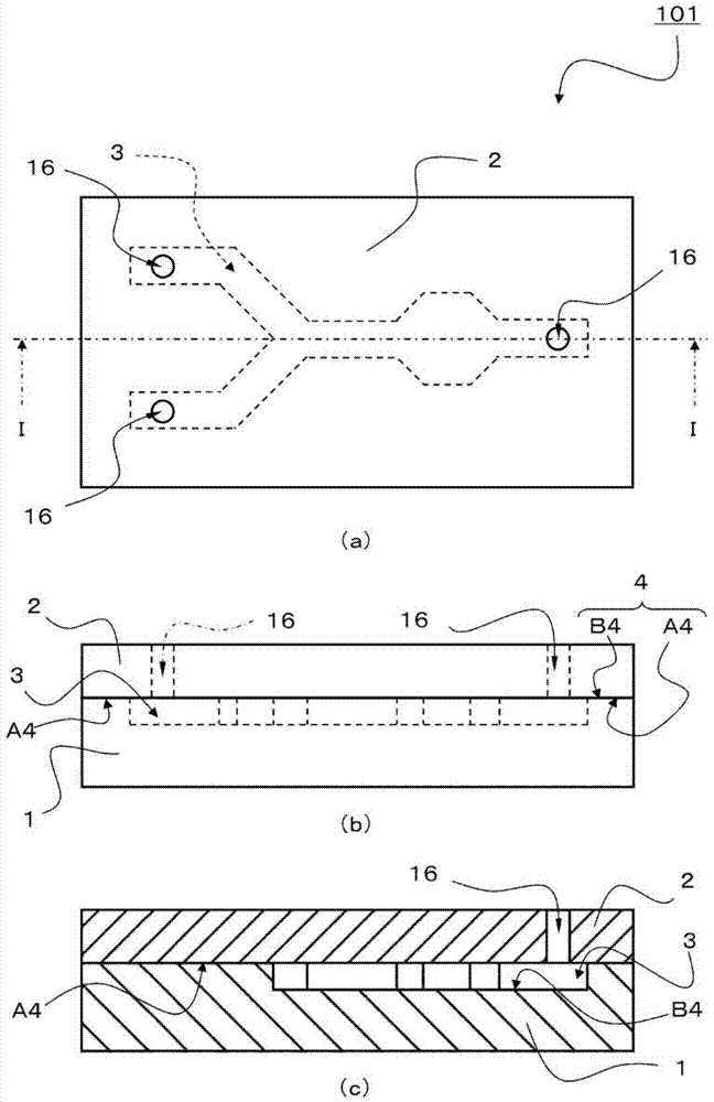
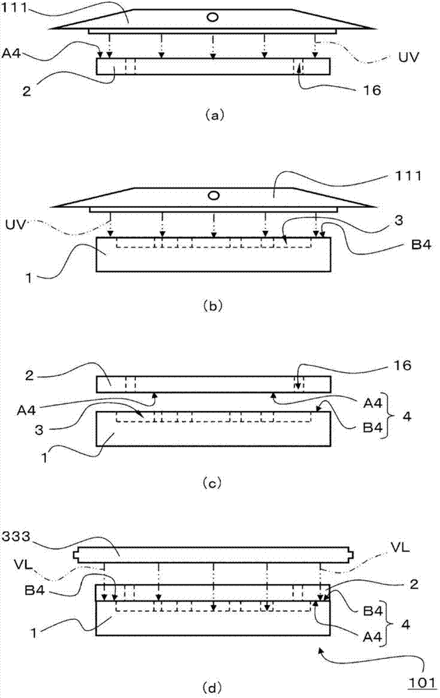
[0035] figure 1 is a diagram illustrating the structure of a microchip 101 manufactured using the manufacturing method of the present invention, figure 1 (a) is a plan view, figure 1 (b) is a side view, figure 1 (c) is figure 1 (a) Cross-sectional view of line I-I. figure 2 It is a figure explaining an example of the manufacturing method of the microchip 101 concerning 1st Embodiment of this invention, figure 2 (a) and figure 2 (b) is a structural diagram showing the ultraviolet light step P11 of irradiating ultraviolet light UV to the light transmissive base material 2 and the resin base material 1, figure 2 (c) is a structural diagram in which the light-transmitting base material 2 before bonding and the resin base material 1 are opposed to each other in the bonding step P12, figure 2 (d) is a structural diagram explaining the visible light process P13 which irradiates the microchip 101 with visible light VL.

[0036] Such as figure 1 As shown, the microch...

Embodiment 1

[0048] Next, the first embodiment of the present invention will be described in more detail through Example 1. The present invention is not limited to the Examples shown below.

[0049] First, as the resin substrate 1 and the light-transmitting substrate 2, a pair of resin substrates (70 mm×20 mm, thickness 2 mm) composed of a cycloolefin polymer (manufactured by Nippon Zeon Co., Ltd., ZEONEX330R, glass transition point 123° C.) were used. The concave portion 3 of the resin base material 1 and the injection hole 16 of the light-transmitting base material 2 are produced by machining the resin base material, respectively.

[0050] Next, the surfaces of the opposing surface B4 of the resin base material 1 and the opposing surface A4 of the light-transmitting base material 2 are irradiated with ultraviolet rays by a Xe excimer lamp (USHIO INC., UER20-172A). Light UV (wavelength 172nm). The irradiation of ultraviolet light UV was carried out in the air, the distance between the l...

no. 2 approach

[0063] Image 6 It is a figure explaining an example of the manufacturing method of the microchip 201 concerning 2nd Embodiment of this invention, Image 6 (a) and Image 6 (b) is a structural diagram showing an ultraviolet light step PU1 for irradiating ultraviolet light UV to a pair of resin substrates, Image 6 (c) and Image 6 (d) is a structural diagram showing a visible light process PV2 in which visible light VL is irradiated to the opposing surfaces 94 of a pair of resin base materials after the ultraviolet light process PU1 is completed, Image 6 (e) is a structural view showing the microchip 201 after the bonding step PA3 is completed. In addition, the same code|symbol is attached|subjected to the same member as 1st Embodiment, and description is abbreviate|omitted.

[0064] The manufacturing method of the microchip 201 according to the second embodiment of the present invention is composed of the following steps: an ultraviolet light step PU1, which irradiates u...


PUM


Abstract

In a method of manufacturing a microchip that has a pair of resin base materials of which facing surfaces are bonded to each other and that has a concave portion formed in at least one of the facing surfaces, the facing surfaces before the pair of resin base materials are bonded to each other are irradiated with ultraviolet light which is light having a wavelength of an ultraviolet region, and the ultraviolet light-irradiated facing surfaces of the pair of resin base materials are irradiated with visible light that substantially includes light having a wavelength of a visible region.

Description

technical field [0001] The present invention relates to a method of manufacturing a microchip used in the fields of chemistry, biochemistry, medicine, etc., the microchip is formed with fine flow paths and circuits, and especially reduces fluorescence. Background technique [0002] In the fields of chemistry, biochemistry, medicine, etc., when it is necessary to carry out chemical reactions, separation, analysis, detection, etc. in the space of fine flow channels, silicon substrates, glass substrates with fine flow paths, etc. are sometimes used. Loop Microchip. However, in the method of microfabrication of inorganic materials such as silicon and glass, the production cost is high and the production time is long, so there are some materials that are not suitable for use in (disposable) applications that are discarded after one use. question. [0003] Therefore, in Patent Document 1, it is proposed that Figure 9 A method of manufacturing a microchip using a pair of resin s...

Claims


Application Information

Patent Timeline
Patent Type & Authority Applications(China)
IPC IPC(8): B01J19/00B81C3/00G01N37/00
CPCB01J19/00B32B37/06G01N37/00B81C3/00B01L3/502707B01L2300/0816B01L2300/0867
Inventor 谷口义尚田口好弘杉村博之金永钟
Owner ALPS ALPINE CO LTD
Features
  • R&D
  • Intellectual Property
  • Life Sciences
  • Materials
  • Tech Scout
  • Unparalleled Data Quality
  • Higher Quality Content
  • 60% Fewer Hallucinations
Learn More