Semiconductor package and manufacturing method of semiconductor package
A manufacturing method and semiconductor technology, applied in semiconductor/solid-state device manufacturing, semiconductor devices, semiconductor/solid-state device components, etc., can solve problems such as scribing knife wear and achieve the effect of reducing maintenance frequency
- Summary
- Abstract
- Description
- Claims
- Application Information
AI Technical Summary
Problems solved by technology
Method used
Image

Examples
Embodiment approach 1
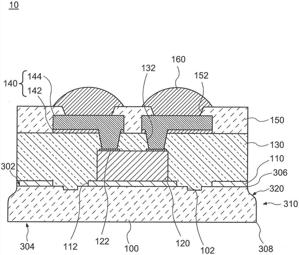
[0058] refer to figure 1 , the outline of the semiconductor package according to Embodiment 1 of the present invention will be described in detail. figure 1 It is a schematic cross-sectional view of a semiconductor package according to one embodiment of the present invention.
[0059] (Structure of semiconductor package 10)
[0060] Such as figure 1 As shown, the semiconductor package 10 has a supporting substrate 100 , an adhesive layer 110 , a semiconductor device 120 , a first resin insulating layer 130 , wiring 140 , a second resin insulating layer 150 and solder balls 160 .
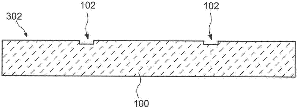
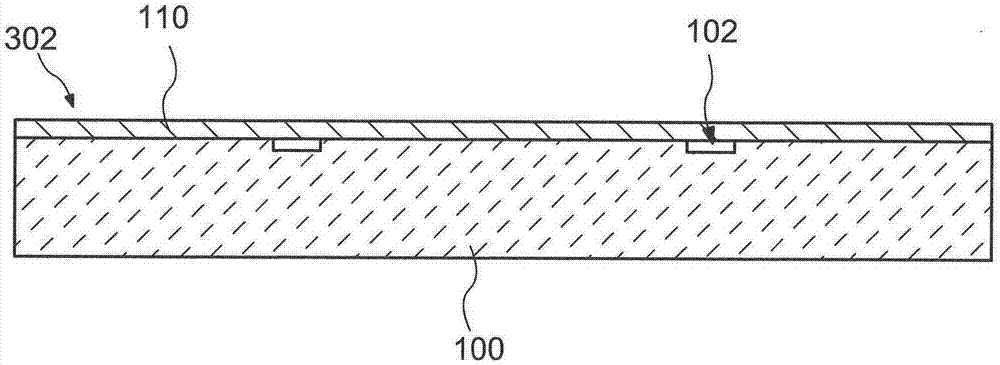
[0061] The support base 100 has a first surface 302 on which the semiconductor device 120 is disposed, a second surface 304 opposite to the first surface, and a side surface 310 between the first surface 302 and the second surface 304 . The first face 302 has a first end 306 at its end and the second face 304 has a second end 308 at its end. The side surface 310 is a surface connecting the first ...
Embodiment approach 2
[0118] refer to Figure 24 , the outline of the semiconductor package according to Embodiment 2 of the present invention will be described in detail. Figure 24 It is a schematic cross-sectional view of a semiconductor package according to one embodiment of the present invention.
[0119] (Structure of semiconductor package 20)
[0120] The semiconductor package 20 of the second embodiment is similar to the semiconductor package 10 of the first embodiment, but differs from the semiconductor package 10 in that the alignment mark 114 is realized by the opening provided in the adhesive layer 110 . In the semiconductor package 20 , no concave portion is formed in the support base 100 . However, similarly to the semiconductor package 10 , a concave portion may be provided on the first surface 302 of the support base 100 of the semiconductor package 20 and an auxiliary alignment mark may be formed. Since other components of the semiconductor package 20 are the same as those of th...
Embodiment
[0131] Hereinafter, the observation result of the optical microscope image of the Example which shows the manufacturing method of the semiconductor package concerning embodiment of this invention is demonstrated. Specifically, as Figure 22 and Figure 23 As shown, a sample separated by the manufacturing method of the embodiment of the present invention and a sample separated by the manufacturing method of the comparative example were compared.
[0132] Figure 30A and Figure 30B It is a diagram showing an optical microscope image comparing the side shape of the support base material in one example of the present invention with the side shape of the support base material in the comparative example. Figure 30A Part (a) of the embodiment is carried out through two steps of scribing of the resin insulating layer (adhesive layer 110, first resin insulating layer 130 and second resin insulating layer 150) and laser irradiation of the supporting substrate 100. Optical microsco...
PUM
 Abstract
Description
Claims
Application Information