SRAM-type FPGA device single-particle inversion detection and error correction circuit

A single-event inversion and circuit technology, applied in the direction of logic circuits using specific components, logic circuits, logic circuits using basic logic circuit components, etc., can solve the problems of increasing chip costs, achieve small chip area and cost, reduce The effect of single event reversal and the realization of anti-SEU function

Active Publication Date: 2017-01-04
GOWIN SEMICON CORP LTD
View PDF4 Cites 6 Cited by
  • Summary
  • Abstract
  • Description
  • Claims
  • Application Information

AI Technical Summary

Problems solved by technology

The end result is the same increase in chip cost as method two

Method used


Image

  • SRAM-type FPGA device single-particle inversion detection and error correction circuit
  • SRAM-type FPGA device single-particle inversion detection and error correction circuit
  • SRAM-type FPGA device single-particle inversion detection and error correction circuit

Examples


Embodiment Construction

[0043] The present invention will be further described below in conjunction with the accompanying drawings, but the embodiments of the present invention are not limited thereto.

[0044] Figure 4 It shows a typical FPGA programming SRAM array (write operation) and its programming verification (read operation) circuit: it is mainly composed of programming control module, address pointer shift register group module, and data shift register group module.

[0045] The programming control module includes an IO interface for external control of chip programming and verification, control state machine (including JTAG TAP control state machine and non-standard serial and parallel programming control state machine), address pointer shift register, Control circuits for data shift registers, boundary scan (Boundary Scan) registers and other shift register groups.

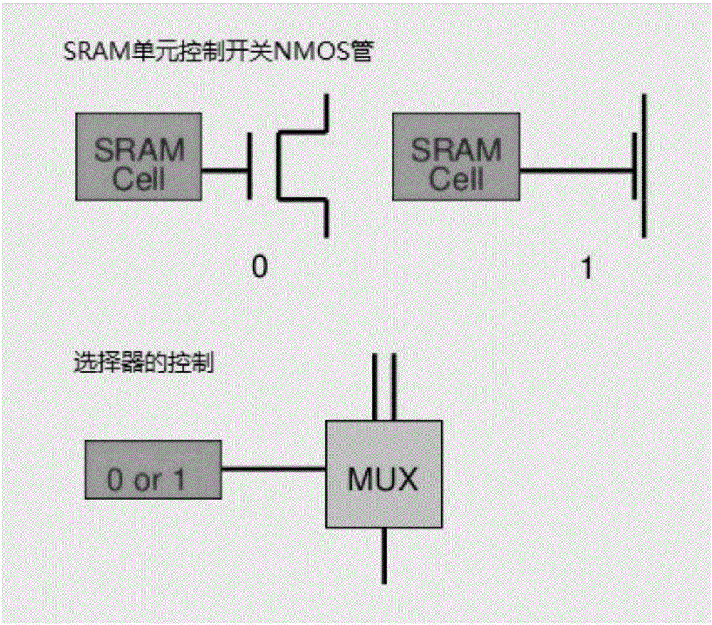
[0046] The address pointer shift register group module includes a shift register and a SRAM word line (Word Line) driver, ...


PUM


Abstract

The present invention discloses an SRAM-type FPGA device single-particle inversion detection and error correction circuit. The SRAM-type FPGA device comprises an SRAM, a programming control module, an address pointer shift register block module and a data shift register block module. The address pointer shift register block module and the data shift register block module are connected with the SRAM; the address pointer shift register block module and the data shift register block module are connected with the programming control module; the programming control module is provided with an address counter and adds an single-particle inversion detection work mode at the programming control module; and a verification detection module is arranged on the loop of the data shift register block module and the programming control module. Through adoption of the existing FPGA programming circuit and based on the SEU detection and error correction circuit, the SRAM-type FPGA device single-particle inversion detection and error correction circuit can effectively realize the anti-SEU function on the basis of increasing little chip area and cost. The speed of the error correction time is fast in the third mode so as to greatly reduce the single-particle inversion influence on the normal work of the device.

Description

technical field [0001] The invention relates to the technical field of programmable logic devices, and more specifically, to a circuit for single event reversal (SEU) detection and error correction of an SRAM FPGA device. Background technique [0002] Programmable logic devices in the field of integrated circuits have become ubiquitous only half a century after the development of integrated circuits, and computers, mobile phones and other digital appliances have become an indispensable part of the structure of modern society. That's because modern computing, communication, manufacturing and transportation systems, including the Internet, all rely on the existence of integrated circuits. [0003] There are many ways to classify integrated circuits, which can be divided into memory (Memory), microprocessor (CPU), custom circuits (ASICs) and programmable logic devices according to their functions. Programmable logic devices can be divided into SPLD, CPLD, FPGA. Midterm FPGAs ...

Claims


Application Information

Patent Timeline
Patent Type & Authority Applications(China)
IPC IPC(8): H03K19/003H03K19/177
CPCH03K19/0033H03K19/17764Y02D10/00
Inventor 朱璟辉高三达
Owner GOWIN SEMICON CORP LTD
Why Eureka
Try Eureka