

Method for manufacturing outer-layer line by using hard board with large drop
A technology of outer layer circuit and production method, which is applied in the fields of printed circuit manufacturing, printed circuit, photolithography/patterning, etc., can solve the problems of poor quality of the outer layer circuit of hard board, reduce bonding instability and increase yield Effect
- Summary
- Abstract
- Description
- Claims
- Application Information
AI Technical Summary
Problems solved by technology
Method used
Image

Examples
Embodiment 1
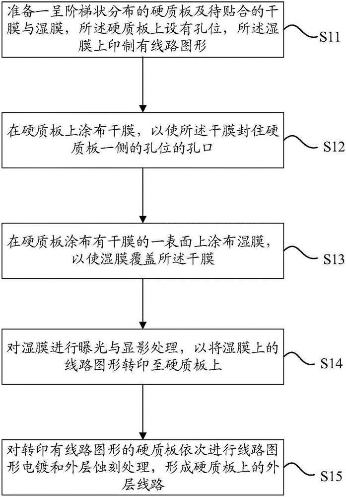
[0026] Please refer to figure 1 , the invention provides a method for manufacturing an outer layer circuit of a hard board with a large drop, comprising the following steps:
[0027] Step S11 , preparing a hard board distributed in a step shape and a dry film and a wet film to be bonded, the hard board is provided with holes, and the wet film is printed with a circuit pattern. Specifically, the hard plate can be a thick copper plate. The drop at the step of the thick copper plate is greater than 0.15mm, and the strength on the dry film is better, which is used for sealing holes and has strong anti-plating ability, while the wet film has better flow It can be used to fill the drop on the hard board. Of course, the hard board in this embodiment has undergone pre-treatment of the outer layer, such as drilling, cleaning, and surface polishing, so as to facilitate the sticking of the dry film and the wet film. It should be pointed out that, in this embodiment, when the surface of...
Embodiment 2
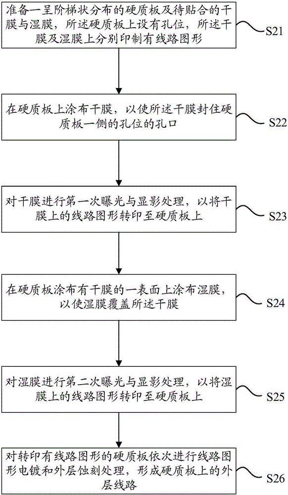
[0040] Please refer to figure 2 , the invention provides a method for manufacturing an outer layer circuit of a hard board with a large drop, comprising the following steps:
[0041] Step S21 , preparing a hard board distributed in a step shape and a dry film and a wet film to be laminated, the hard board is provided with holes, and circuit patterns are printed on the dry film and the wet film respectively. Specifically, the hard plate can be a thick copper plate. The drop at the step of the thick copper plate is greater than 0.15mm, and the strength on the dry film is better, which is used for sealing holes and has strong anti-plating ability, while the wet film has better flow It can be used to fill the drop on the hard board. Of course, the hard board in this embodiment has undergone pre-treatment of the outer layer, such as drilling, cleaning, and surface polishing, so as to facilitate the sticking of the dry film and the wet film. It should be pointed out that, in this...
PUM
| Property | Measurement | Unit |
|---|---|---|
| Thickness | aaaaa | aaaaa |
| Thickness | aaaaa | aaaaa |
| Concentration | aaaaa | aaaaa |
Abstract
Description
Claims
Application Information