

Prebias switch machine circuit and prebias circuit and method of multi-cascade converter
A switch circuit, pre-bias technology, applied in the direction of adjusting electrical variables, converting DC power input to DC power output, instruments, etc., can solve the problems of easy damage to circuit devices, complex control of DC converters, and difficult control of switching points, etc. problem, to achieve the effect of preventing falling, realizing simplicity and precise control
- Summary
- Abstract
- Description
- Claims
- Application Information
AI Technical Summary
Problems solved by technology
Method used
Image

Examples
Embodiment 1
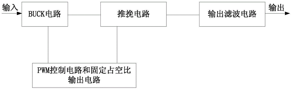
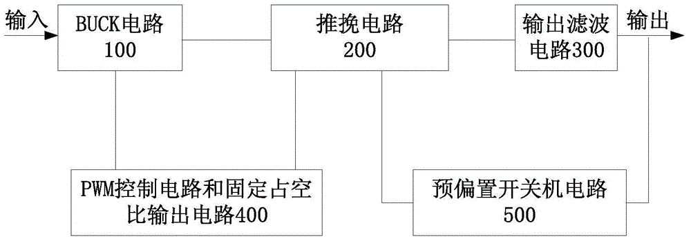
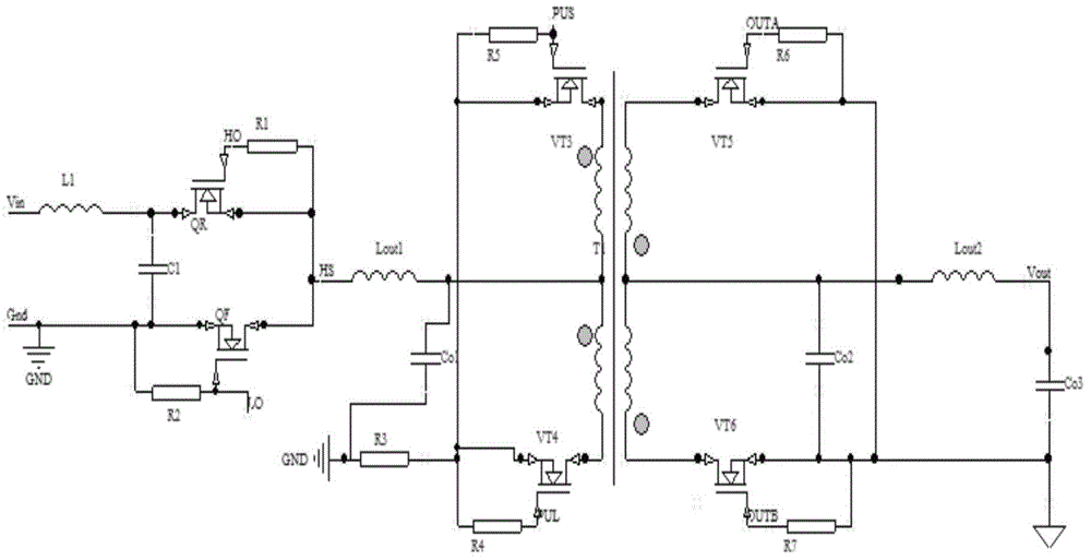
[0035] This embodiment provides a schematic structural diagram of a multi-cascade converter pre-bias circuit, as shown in figure 2 As shown, in this embodiment, a multi-cascade converter is taken as an example for illustration. The multi-cascade converter pre-bias circuit of the present invention includes a BUCK circuit 100, a push-pull circuit 200, an output filter circuit 300, a PWM control circuit and The fixed duty cycle output circuit 400 and the pre-bias switch machine circuit 500 . One end of the pre-bias switch circuit 500 is connected to the output end of the output filter circuit 300 , and the other end is connected to the push-pull circuit 200 . The BUCK circuit 100 adopts the synchronous rectification technology, and the push-pull circuit 200 also adopts the synchronous rectification technology for the secondary side rectification. Such as image 3 As shown, the BUCK circuit 100 includes a rectifier switch tube QR, a freewheeling switch tube QF, a first inductor...
Embodiment 2
[0041] This embodiment provides a pre-bias switch circuit, such as image 3 As shown, when the pre-bias detection circuit detects that the output SENSE voltage has reached the set value. The high level is output by the comparison circuit to enable the D2 driver chip. The characteristic of the D2 driver chip is that only when the EN signal is high, the input signals of INA and INB can be transmitted to OUTA and OUTB. When the pre-bias detection circuit detects that the output voltage has reached the set value, the driving signals of INA and INB are sent to OUTA and OUTB. Thus, the drive of the secondary side rectification MOS tube is turned on to achieve the purpose of preventing backfeeding. When D1A outputs a high level, through R11, the voltage of pin 3 of D1A is raised to eliminate the disturbance. When the output voltage drops to a certain set value, D1A outputs a low level, the D2 driver chip stops working, and the secondary side rectifier MOS tube driver is turned off...
Embodiment 3
[0043] This embodiment provides a pre-bias switch circuit, such as Figure 4 As shown, when the pre-bias detection circuit detects that the VOUT output voltage has reached the set value. The high level is output by the comparison circuit to enable the D2 driver chip. The characteristic of the D2 driver chip is that only when the EN signal is high, the input signals of INA and INB can be transmitted to OUTA and OUTB. When the pre-bias detection circuit detects that the output voltage has reached the set value, the driving signals of INA and INB are sent to OUTA and OUTB. Thus, the drive of the secondary side rectification MOS tube is turned on to achieve the purpose of preventing backfeeding. When D1A outputs a high level, through R11, the voltage of pin 3 of D1A is raised to eliminate the disturbance. When the output voltage drops to a certain set value, D1A outputs a low level, the D2 driver chip stops working, and the secondary side rectifier MOS tube driver is turned off...
PUM
 Abstract
Description
Claims
Application Information