Array substrate, driving method, liquid crystal display panel and display device

An array substrate and a technology for displaying brightness, which are applied in the fields of liquid crystal display panels, array substrates and driving methods, and display devices, can solve the problem of uneven display brightness of pixels, and achieve the effect of improving display brightness.

Pending Publication Date: 2017-01-18
HEFEI BOE OPTOELECTRONICS TECH +1
View PDF5 Cites 7 Cited by
  • Summary
  • Abstract
  • Description
  • Claims
  • Application Information

AI Technical Summary

Problems solved by technology

[0005] Embodiments of the present application provide an array substrate, a driving method, a liquid crystal display ...

Method used


Image

  • Array substrate, driving method, liquid crystal display panel and display device
  • Array substrate, driving method, liquid crystal display panel and display device
  • Array substrate, driving method, liquid crystal display panel and display device

Examples


Embodiment 1

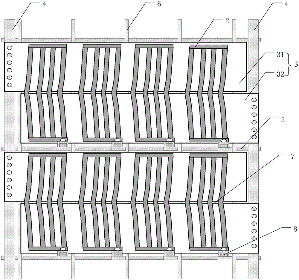
[0039] see figure 1 , an array substrate provided in Embodiment 1 of the present application, comprising: common electrode groups arranged in different layers (not in figure 1 Marked in) and pixel electrode 2.

[0040] Wherein, the pixel electrode 2 is a pixel electrode with a single pixel double domain structure.

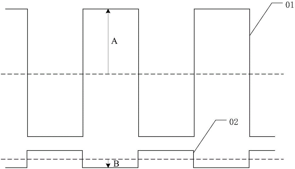
[0041] The common electrode group is divided into common electrodes 3 in multiple areas that are not connected: the adjacent pixel electrodes of the same domain with the highest display brightness in the same gray scale correspond to the common electrode 31 in the same area in the common electrode group, and are in the same gray scale The common electrode 31 of each area with the highest display brightness is loaded with a constant voltage signal (for example: DC voltage signal); the common electrode 32 of other areas in the common electrode group is loaded with a complex voltage signal with a preset amplitude based on the constant voltage signal (For example, it...

Embodiment 2

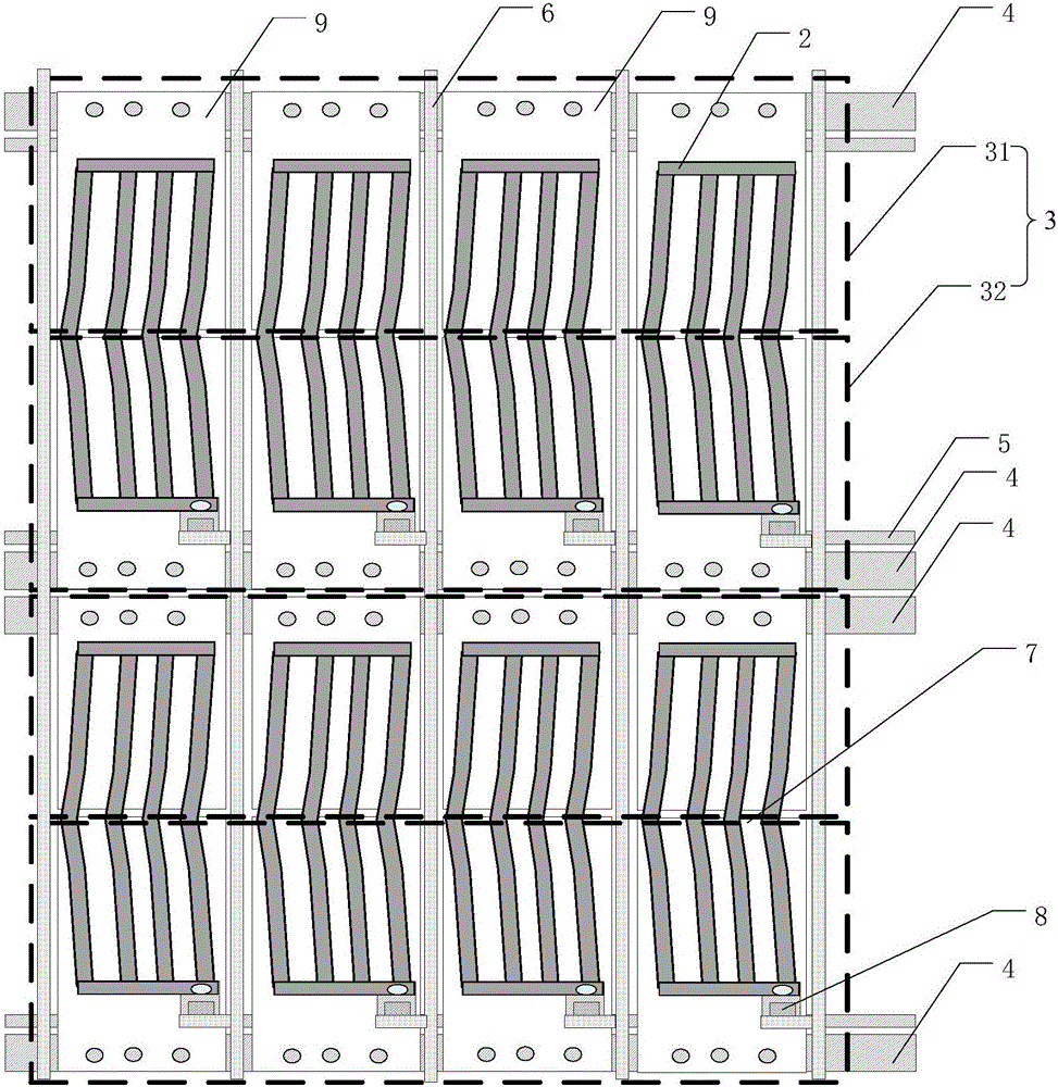
[0053] see image 3 , image 3 An array substrate provided in Embodiment 2 of the present application is similar to the array substrate provided in Embodiment 1 of the present application, and the same parts will not be repeated here, and only the different parts will be described below.

[0054] The common electrode 3 (such as figure 2 The common electrode 9 is divided into disjoint sub-regions according to the pixel unit.

[0055] Since the common electrodes 9 in each area 3 are divided into the common electrodes 9 in disjoint sub-areas according to the pixel unit, no matter what kind of pixel array polarity inversion method is used for the array substrate, the technical solution provided by the embodiment of the present application is the same. Be applicable.

[0056] Preferably, if image 3 As shown, the array substrate provided in Embodiment 2 of the present application also includes a plurality of common electrode lines 4 for transmitting voltage signals to the comm...

Embodiment 3

[0062] see Figure 4 , Figure 4 An array substrate provided in Embodiment 3 of the present application is similar to the array substrate provided in Embodiment 1 of the present application, and the same parts will not be repeated here, and only the different parts will be described below.

[0063] In the array substrate provided in the third embodiment of the present application, the pixel electrode 2 is a pixel electrode with a double-pixel double-domain structure.


PUM


Abstract

The invention provides an array substrate, a driving method, a liquid crystal display panel and a display device, and aims to solve the problem that the display brightness of pixel is not the same under a same gray level. The array substrate provided by the invention comprises a public electrode group and pixel electrodes, wherein the public electrode group and the pixel electrodes are arranged on different layers; the pixel electrodes are pixel electrodes of a dual-domain structure at least; the public electrode group comprises public electrodes of a plurality of areas which are not connected; adjacent same-domain pixel electrodes with the highest display brightness at a same gray level correspond to public electrodes in a same area, of the public electrode group; public electrodes with the highest display brightness in different areas, at a same gray level, are loaded with constant voltage signals; public electrodes in other areas, of the public electrode group, are loaded with complex voltage signals which adopt the constant voltage signals as reference and have preset vibration amplitudes.

Description

technical field [0001] The present application relates to the field of display technology, in particular to an array substrate and a driving method, a liquid crystal display panel, and a display device. Background technique [0002] Thin Film Transistor Liquid Crystal Display (TFT-LCD) has the characteristics of small size, low power consumption, and no radiation, and occupies a dominant position in the current flat panel display market. Wide viewing angle display technology has become a research hotspot at present. [0003] Wide viewing angle liquid crystal displays can be classified into: In Plane Switching (IPS) type and Advanced Super Dimension Switch (Advanced Super Dimension Switch, ADS) type according to display modes. Among them, the ADS mode liquid crystal display forms a multidimensional electric field through the electric field generated by the edge of the slit electrode in the same plane in the liquid crystal display and the electric field generated between the ...

Claims


Application Information

Patent Timeline
IPC IPC(8): G02F1/1343G09G3/36
CPCG02F1/134309G09G3/3648
Inventor 马俊才
Owner HEFEI BOE OPTOELECTRONICS TECH
Why Eureka
Try Eureka