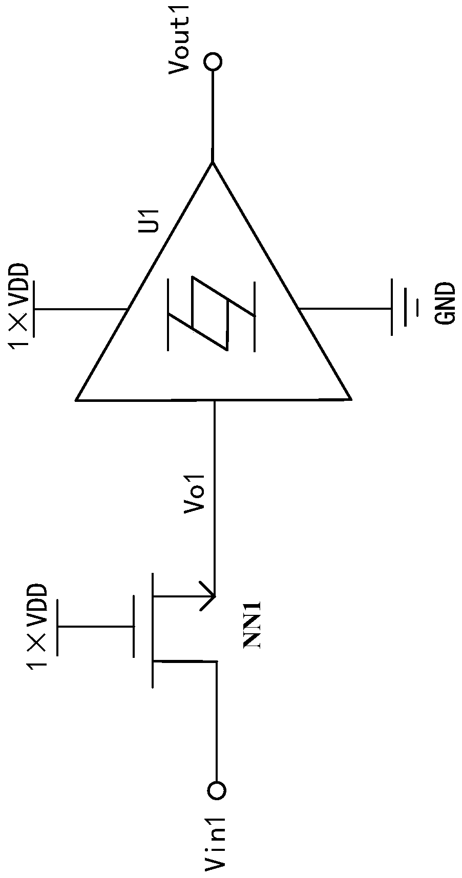
level shift circuit
A technology of level shifting circuit and flipping circuit, applied in the direction of logic circuit, logic circuit connection/interface layout, electrical components, etc., can solve the problems of large duty cycle, distortion, insufficient, etc., and achieve the ability to avoid glitches and anti-jitter The effect of strong and strong anti-burr ability
- Summary
- Abstract
- Description
- Claims
- Application Information
AI Technical Summary
Problems solved by technology
Method used
Image
Examples
Embodiment 1
[0026] Such as Figure 6 As shown, the level shift circuit of this embodiment includes a Schmitt trigger 3 , a native NMOS transistor NN3 and an inverter INV2 . Wherein, the Schmitt trigger 3 includes a transmission high voltage module 31, a transmission low voltage module 32 and a flipping circuit 33, the input end of the transmission high voltage module 31 and the input end of the transmission low voltage module 32 are respectively electrically connected to the voltage signal input end . The output end of the transmission high voltage module 31 sends a high voltage signal to the inversion circuit 33 , and the output end of the transmission low voltage module 32 sends a low voltage signal to the inversion circuit 33 . The high-voltage signal is a part of the signal from VDD to 2×VDD in the input signal Vin3, and the low-voltage signal is a part of the signal from 0 to VDD in the input signal Vin3. The flipping circuit 33 outputs a square wave signal Vo4 according to the hig...
Embodiment 2
[0037] Such as Figure 7 As shown, the level shift circuit of this embodiment includes a Schmitt trigger 4, a native NMOS transistor NN4 and an inverter INV3. The Schmitt trigger 4 includes a transmission high voltage module 41 , a transmission low voltage module 42 and an inversion circuit 43 , the input terminals of the transmission high voltage module 41 and the transmission low voltage module 42 are respectively electrically connected to the voltage signal input terminals. The output end of the transmission high voltage module 41 sends a high voltage signal to the inversion circuit 43 , and the output end of the transmission low voltage module 42 sends a low voltage signal to the inversion circuit 43 . The high-voltage signal is part of the signal from VDD to 2×VDD in the input signal Vin4, and the low-voltage signal is part of the signal from 0 to VDD in the input signal Vin4. The inversion circuit 43 outputs a square wave signal Vo5 according to the high voltage signal ...
PUM
 Abstract
Description
Claims
Application Information


