

Array substrate, display panel including same, and display device
An array substrate and display panel technology, applied in the input/output process of data processing, instruments, calculations, etc., can solve the problems of poor touch detection accuracy, large resistance value, and decreased touch detection accuracy of touch screens, and achieve improved touch The effect of detecting accuracy, reducing effective resistance, and improving uniformity
- Summary
- Abstract
- Description
- Claims
- Application Information
AI Technical Summary
Problems solved by technology
Method used
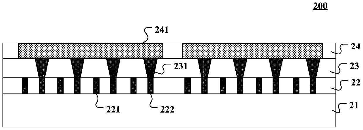
Image

Examples
Embodiment Construction
[0018] The application will be further described in detail below in conjunction with the accompanying drawings and embodiments. It should be understood that the specific embodiments described here are only used to explain related inventions, rather than to limit the invention. It should also be noted that, for the convenience of description, only the parts related to the related invention are shown in the drawings.
[0019] It should be noted that, in the case of no conflict, the embodiments in the present application and the features in the embodiments can be combined with each other. The present application will be described in detail below with reference to the accompanying drawings and embodiments.
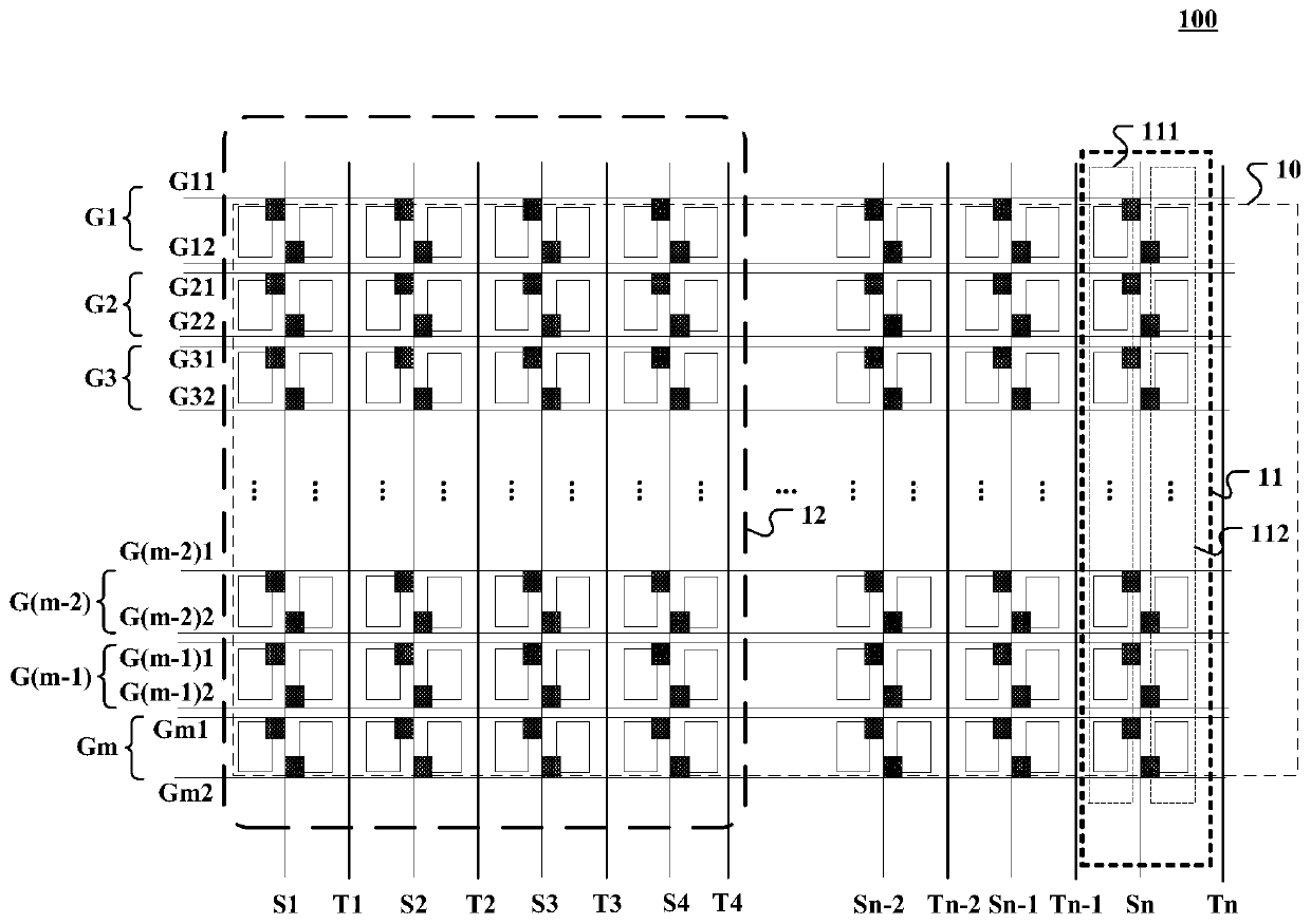
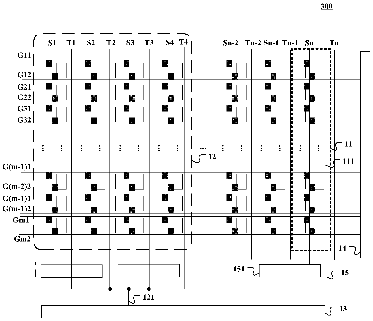
[0020] Please refer to figure 1 , which shows a schematic structural diagram of an embodiment of the array substrate provided by the present application.
[0021] In this embodiment, the array substrate 100 includes a base substrate, a pixel array 10 formed on the base subs...
PUM
 Abstract
Description
Claims
Application Information