Electrostatic discharge protection device and operation method thereof

An electrostatic discharge protection and electrical technology, applied in the field of electrostatic discharge protection devices, can solve the problems of reducing the effective resistance of electrostatic discharge protection devices, parasitic silicon-controlled rectifiers cannot be turned on smoothly, etc.

Pending Publication Date: 2022-07-29
MACRONIX INT CO LTD
View PDF0 Cites 0 Cited by
  • Summary
  • Abstract
  • Description
  • Claims
  • Application Information

AI Technical Summary

Problems solved by technology

[0005] The invention relates to an electrostatic discharge protection device and its operating method, which can solve the problem that known parasitic silicon-controlled rectifiers cannot be opened smoothly, and can reduce the effective resistance of the electrostatic discharge protection device

Method used


Image

  • Electrostatic discharge protection device and operation method thereof
  • Electrostatic discharge protection device and operation method thereof
  • Electrostatic discharge protection device and operation method thereof

Examples


no. 1 example

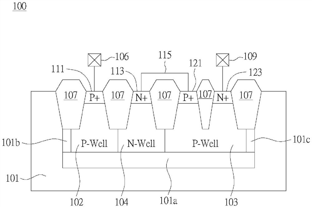
[0038] Please refer to Figure 1A and Figure 1B , which respectively show a cross-sectional schematic diagram of the electrostatic discharge protection device 100 according to an embodiment of the present invention and a schematic diagram of an equivalent circuit thereof.

[0039] According to an embodiment of the present invention, the ESD protection device 100 includes a semiconductor substrate 101 , a first well region 102 , a second well region 103 , a third well region 104 , a first doped region 111 , and a second doped region 113 , the third doped region 121 and the fourth doped region 123 .

[0040] In one embodiment, the semiconductor substrate 101 may be made of any suitable base semiconductor (eg, crystalline silicon or germanium), compound semiconductors (eg, silicon carbide, gallium arsenide, gallium phosphide, iodine phosphide, iodine arsenide, and / or antimony iodine) or a combination of the above. The semiconductor substrate 101 is, for example, a P-type sub...

no. 2 example

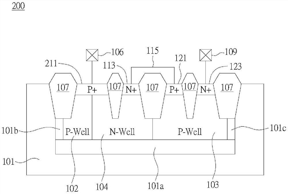
[0049] Please refer to Figure 2A and Figure 2B , which respectively show a cross-sectional schematic diagram of an electrostatic discharge protection device 200 according to another embodiment of the present invention and a schematic diagram of an equivalent circuit thereof. The structure of the ESD protection device 200 is similar to Figure 1A In the structure of the ESD protection device 100 shown, a part of the first doped region 211 is located in the first well region 102 , and another part of the first doped region 211 is located in the third well region 104 . The first doped region 211 is similar to the first doped region 111 .

[0050] In the ESD protection device 200 , there are two parallel diodes, which are coupled through the first well region 102 and the third well region 104 to form a diode 212 , and pass through the first doped region 211 and the third well region 104 Coupled to form another diode 214, thereby increasing the effective circuit path for electr...

no. 3 example

[0055] Please refer to Figure 3A and Figure 3B , which respectively show a cross-sectional schematic diagram of an electrostatic discharge protection device according to another embodiment of the present invention and a schematic diagram of an equivalent circuit thereof. The structure of the ESD protection device 300 is similar to Figure 1A In the structure of the ESD protection device 100 shown, except that a part of the first doped region 311 is located in the first well region 102 , another part of the first doped region 311 is located in the third well region 104 , and the second doped region 313 The third doped region 321 is directly connected to each other to form a junction 316 . The first doping region 311 , the second doping region 313 and the third doping region 321 are similar to the first doping region 111 , the second doping region 113 and the third doping region 121 .

[0056] In the ESD protection device 300 , there are two parallel diodes, which are couple...


PUM


Abstract

The invention discloses an electrostatic discharge protection device and an operation method thereof, and the electrostatic discharge protection device comprises a semiconductor substrate, a first well region, a second well region, a third well region, a first doped region, a second doped region, a third doped region, and a fourth doped region. The first well region, the second well region and the third well region are located in the semiconductor substrate, and the third well region is directly coupled between the first well region and the second well region. The first well region and the second well region have a first electrical property, and the third well region has a second electrical property. The first doped region has a first electrical property and is located in the first well region. The second doped region has a second electrical property and is located in the third well region, and the first doped region and the second doped region are isolated from each other. The third doped region and the fourth doped region have the first electrical property and the second electrical property respectively, are located in the second well region and are isolated from each other, and the second doped region is electrically coupled with the third doped region. The first well region, the second well region, the third well region and the fourth doped region form a parasitic silicon controlled rectifier.

Description

technical field [0001] The present invention relates to a semiconductor device, and more particularly, to an electrostatic discharge protection device and an operation method thereof. Background technique [0002] Electrostatic discharges result from powerful current pulses introduced by high voltage discharges over short periods of time (typically within 100 nanoseconds). Integrated circuits and semiconductor components are quite sensitive to electrostatic discharge. Especially during component mounting, because humans or machines touch the pins, strong current pulses are often passed through the integrated circuit, resulting in component failure. There is therefore a need to provide an effective electrostatic discharge protection device for integrated circuits. [0003] Parasitic Silicon Controlled Rectifier (SCR) is an on-chip semiconductor ESD protection device, which can be turned on by snapback when ESD occurs, conducting ESD current to ground to achieve the protect...

Claims


Application Information

Patent Timeline
Patent Type & Authority Applications(China)
IPC IPC(8): H01L27/02
CPCH01L27/0262H01L27/0296H01L29/861H01L29/87H01L29/0649H01L27/0255H01L29/7436H01L27/0248
Inventor 王世钰徐志纬黄文聪
Owner MACRONIX INT CO LTD
Why Eureka
Try Eureka