

Semiconductor device and process for manufacturing the same
a technology of semiconductor devices and semiconductors, applied in semiconductor devices, semiconductor/solid-state device details, diodes, etc., can solve the problems of difficult flow of large-volume current in the inductor b>9, inability to increase the interconnection width, and deterioration of the inductance characteristics, so as to improve the q value of the inductor, reduce the effect of effective resistance value and large
- Summary
- Abstract
- Description
- Claims
- Application Information
AI Technical Summary
Benefits of technology
Problems solved by technology
Method used
Image

Examples
embodiment 1
Preferred Embodiment 1
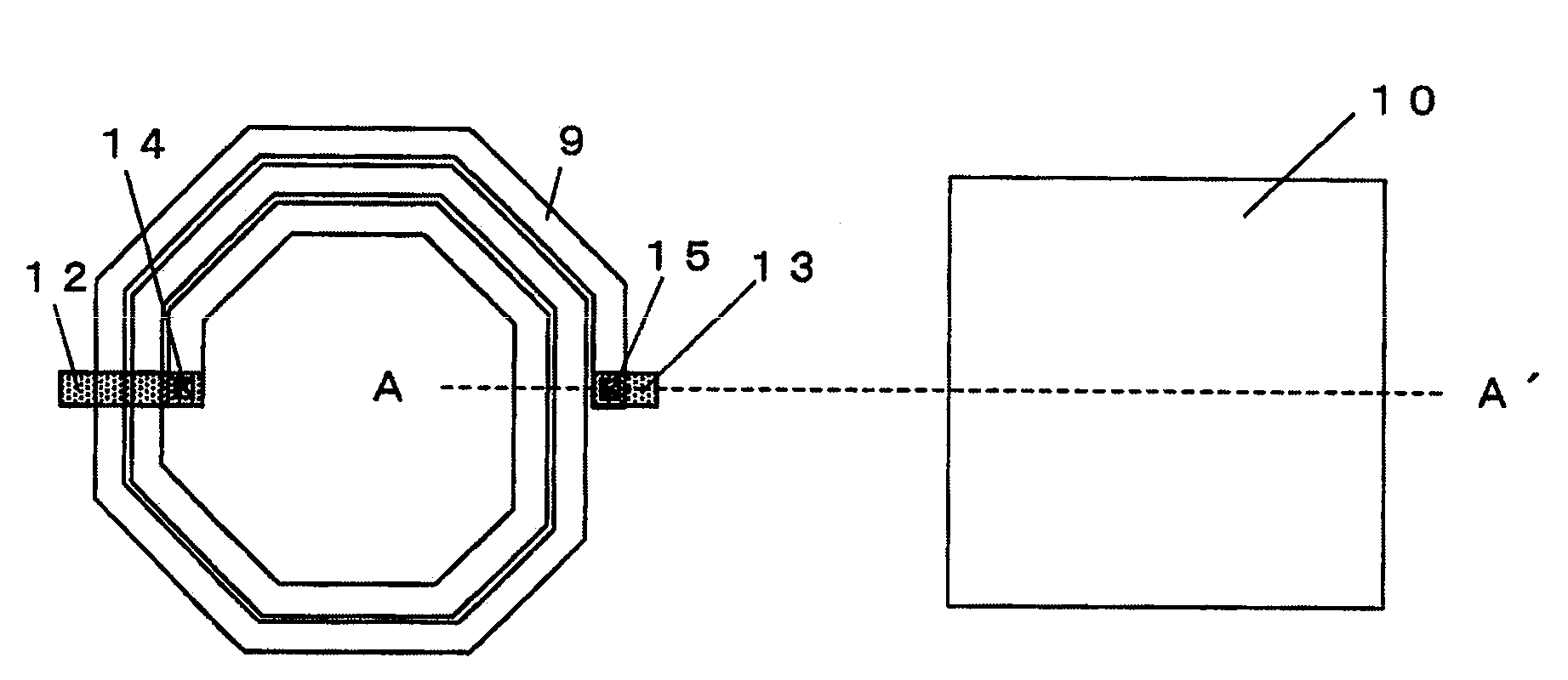
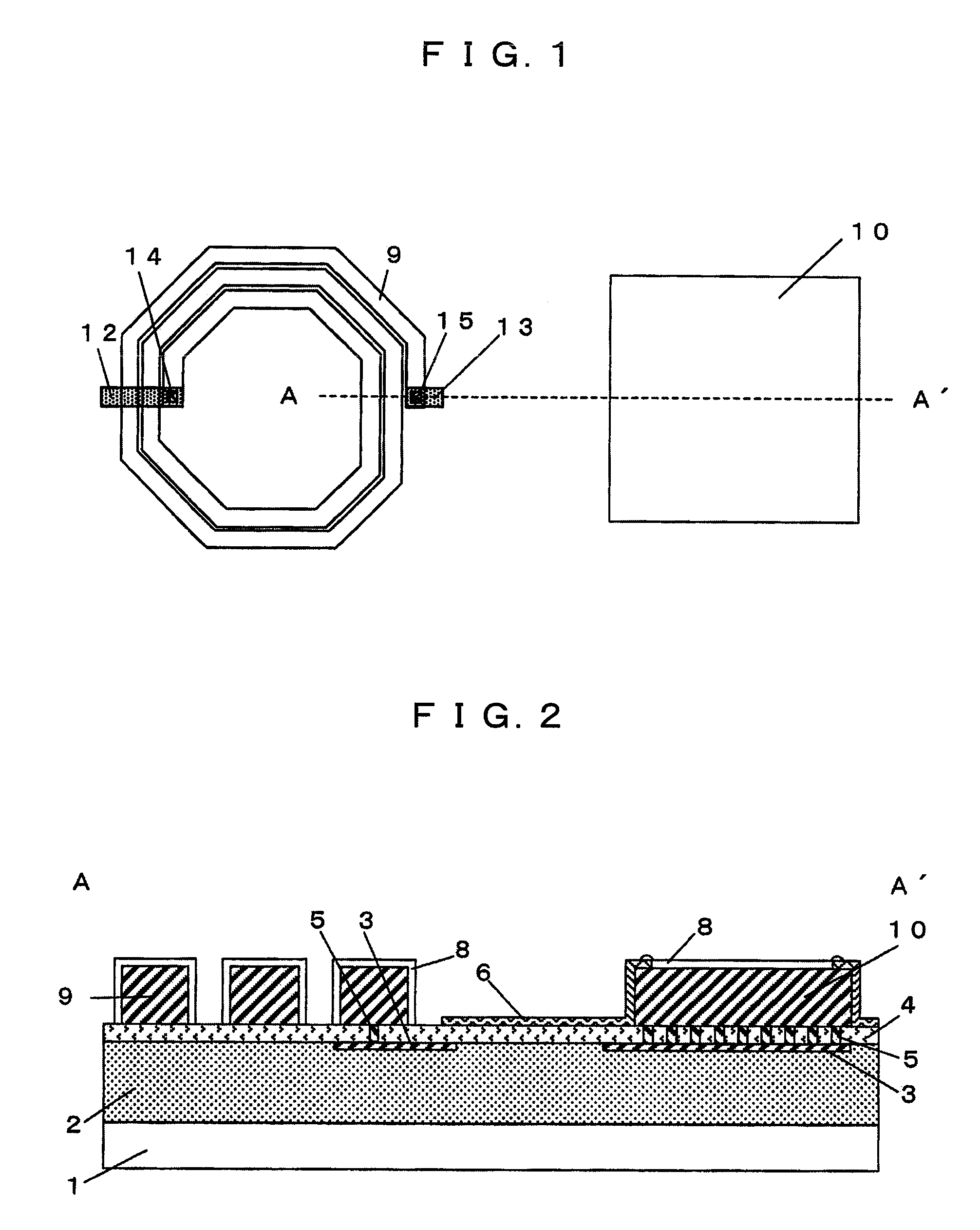
[0046]FIG. 1 is a plain view of a semiconductor device comprising an inductor having a helicoidal shape according to a preferred embodiment 1 of the present invention, and FIG. 2 is a cross sectional view of FIG. 1 taken along the line A-A′. In FIG. 1, 9 denotes an inductor, 10 denotes a conductive pad, 12 denotes drawing interconnection in an inner terminal of the inductor, 13 denotes drawing interconnection in an outer terminal of the inductor, 14 denotes a drawing via hole in the inner terminal of the inductor, and 15 denotes a drawing via hole in the outer terminal of the inductor. In FIG. 2, 1 denotes a semiconductor substrate, 2 denotes an inter-layer insulation film, 3 denotes lower interconnection, 4 denotes an insulation film, 5 denotes a via hole, 6 denotes a protective film which covers the insulation film 4, 8 denotes a plating layer which is an example of conductive thin layers, 9 denotes an inductor, and 10 denotes a conductive pad.
[0047]The insul...
embodiment 2
Preferred Embodiment 2
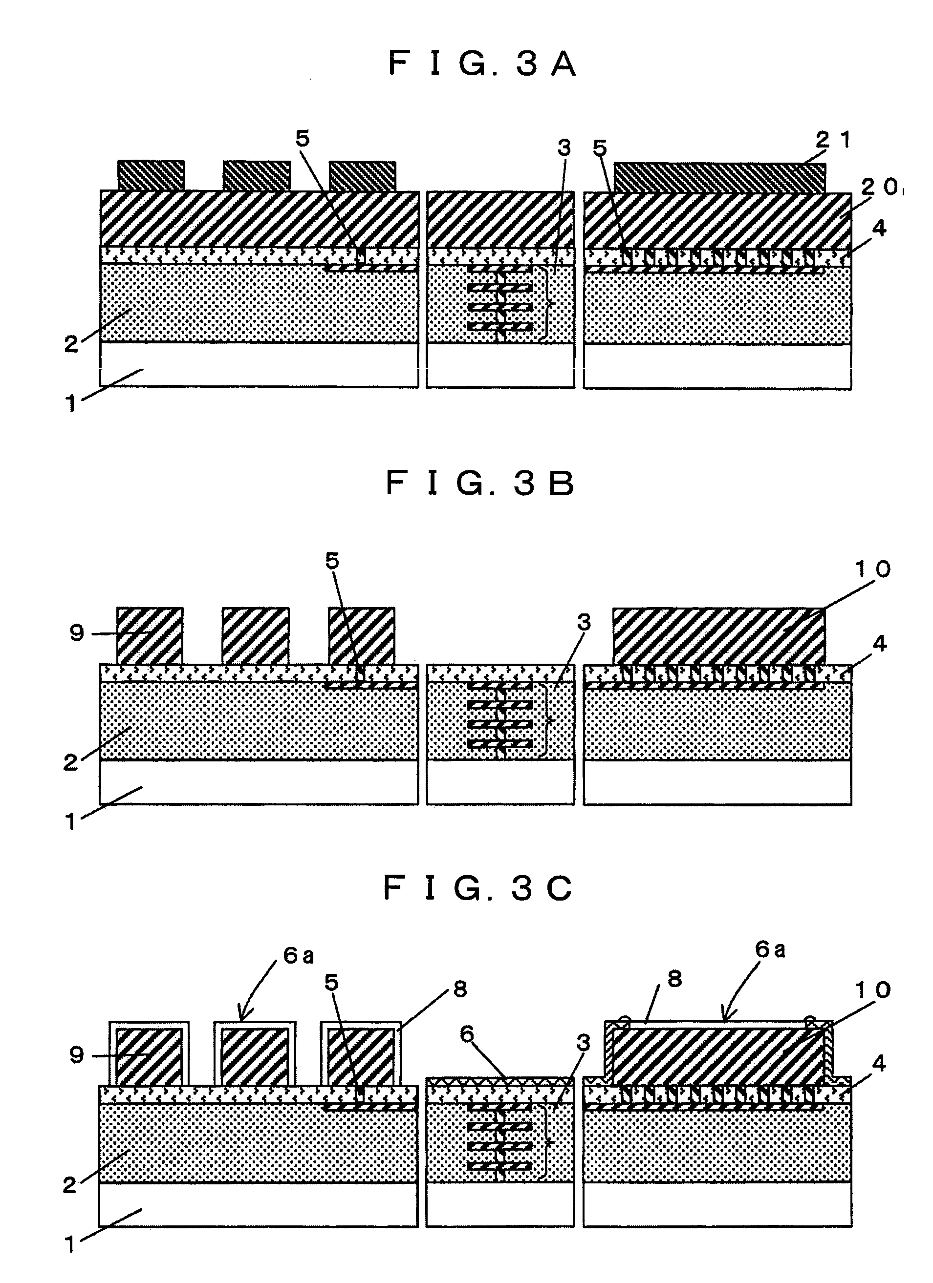
[0049]FIG. 3 are cross sectional views of respective steps in a process for manufacturing an inductor having a helicoidal shape according to a preferred embodiment 2 of the present invention. In FIGS. 3, 1 denotes a semiconductor substrate, 2 denotes an inter-layer insulation film, 3 denotes lower interconnection, 4 denotes an insulation film, 5 denotes a via hole, 6 denotes a protective film, 8 denotes a plating layer which is an example of conductive thin layers, 9 denotes an inductor, and 10 denotes a conductive pad.
[0050]First, the semiconductor substrate 1 provided with the lower interconnection (constituting multilayered interconnection) 3 in the inter-layer insulation film 2 is prepared, and the insulation film 4 is formed on the semiconductor substrate 1. Then, the via holes 5, which will provide an inter-layer connection to the inductor 9 and the conductive pad 10, are formed in the insulation film 4 (see FIG. 3A). Next, a metal film 20 made of aluminu...
embodiment 3
Preferred Embodiment 3
[0054]FIGS. 4 and 5 are cross sectional views of respective steps in a process for manufacturing an inductor having a helicoidal shape according to a preferred embodiment 3 of the present invention. In FIGS. 4 and 5, 1 denotes a semiconductor substrate, 2 denotes an inter-layer insulation film, 3 denotes lower interconnection, 4 denotes an insulation film, 5 denotes a via hole, 6 denotes a protective film, 7 denotes a metal thin film, 8 denotes a plating layer which is an example of conductive thin layers, 9 denotes an inductor, and 10 denotes a conductive pad.
[0055]First, the semiconductor substrate 1 provided with the lower interconnection (constituting multilayered interconnection) 3 in the inter-layer insulation film 2 is prepared, and the insulation film 4 is formed on the semiconductor substrate 1. Then, the via holes 5, which provides an inter-layer connection in the inductor 9 and the conductive pad 10, are formed in the insulation film 4 (see FIG. 4A)....
PUM
| Property | Measurement | Unit |
|---|---|---|
| skin depth | aaaaa | aaaaa |
| thickness | aaaaa | aaaaa |
| thickness | aaaaa | aaaaa |
Abstract
Description
Claims
Application Information