Through silicon via array-based three-dimensional spiral inductor

A spiral inductor and through-silicon via technology, applied in inductors, electrical solid devices, circuits, etc., can solve the problems of limiting the use of inductors, large discrete inductors, and small inductor inductance values.

Inactive Publication Date: 2016-12-07
XIDIAN UNIV
View PDF3 Cites 10 Cited by
  • Summary
  • Abstract
  • Description
  • Claims
  • Application Information

AI Technical Summary

Problems solved by technology

[0004] At present, there are two types of inductors: discrete inductors and integrated inductors. Individual discrete inductors are generally large in size, which is not conducive to monolithic integration and system miniaturization; inductors made

Method used


Image

  • Through silicon via array-based three-dimensional spiral inductor
  • Through silicon via array-based three-dimensional spiral inductor
  • Through silicon via array-based three-dimensional spiral inductor

Examples


Embodiment Construction

[0027] The present invention will be specifically introduced below in conjunction with the accompanying drawings and specific embodiments.

[0028] 1. The structure of three-dimensional spiral inductor

[0029] The structure of the three-dimensional spiral inductor based on the through-silicon hole array of the present invention includes: a top layer, a middle layer and a bottom layer.

[0030] 1. Top floor

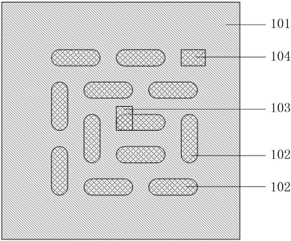
[0031] refer to figure 1 , the top layer is the top dielectric layer 101, which is made of insulating material, and the top metal interconnection 102, the top first plate metal interconnection 103 and the top second plate metal interconnection 104 are made therein.

[0032] The insulating material used for making the top dielectric layer 101 is silicon dioxide, silicon nitride or silicon oxynitride.

[0033] The material used to make the top metal interconnection 102 , the top first plate metal interconnection 103 and the top second plate metal interconnection 104 is c...


PUM


Abstract

The invention discloses a through silicon via array-based three-dimensional spiral inductor, which comprises a top layer, an intermediate layer and a bottom layer, wherein through silicon vias in the intermediate layer are arranged into an N*N square matrix (N is greater than or equal to 5); metal posts in the through silicon vias are connected with top-layer metal interconnection lines on the top layer and bottom-layer metal interconnection lines on the bottom layer to form a series path; the series path is of a three-dimensional spiral structure (namely the three-dimensional spiral inductor) in a vertical plane; current flows to another polar plate from one polar plate of the three-dimensional spiral inductor when the series path is used; and the current sequentially passes through each metal post except for the metal post at the center. An inductance value of each through silicon via is equal to the sum of self-inductance itself and mutual inductance of adjacent through silicon via; and the total inductance value of the three-dimensional spiral inductor is equal to superposition of self-inductance values and mutual inductance values of all through silicon vias in the array, so that the quality and the inductance value of the integrated inductor can be greatly improved by the three-dimensional spiral inductor disclosed by the invention.

Description

technical field [0001] The invention relates to an inductor, in particular to a three-dimensional spiral inductor based on a through-silicon via (TSV) array, and belongs to the field of integrated inductors oriented to radio frequency / microwave integrated circuits. Background technique [0002] As one of the three major passive devices, inductors are an important part of various circuits in modern communication systems. They are widely used in analog, analog-digital hybrid, radio frequency and microwave integrated circuits. It also has the functions of screening signals, filtering noise, stabilizing current and suppressing electromagnetic wave interference. [0003] The most common usage of inductors in circuits is to form LC filter circuits together with capacitors. [0004] At present, there are two types of inductors: discrete inductors and integrated inductors. Individual discrete inductors are generally large in size, which is not conducive to monolithic integration an...

Claims


Application Information

Patent Timeline
IPC IPC(8): H01L23/64
CPCH01L28/10
Inventor 尹湘坤朱樟明杨银堂李跃进丁瑞雪
Owner XIDIAN UNIV
Why Eureka
Try Eureka