Stack inductor with different metal thickness and metal width

a technology of inductor and metal thickness, applied in the field of microelectronics, can solve the problems of not meeting the requirements of circuit design, reducing q factor and self-resonance frequency, etc., and achieves the effect of increasing the inductance value, reducing the resistance of the bottom metal, and widening the metal width

Active Publication Date: 2013-05-14
SHANGHAI HUAHONG GRACE SEMICON MFG CORP
View PDF19 Cites 11 Cited by
  • Summary
  • Abstract
  • Description
  • Claims
  • Application Information

AI Technical Summary

Benefits of technology

[0008]The advantages of this invention are: with this invention can increase inductance value at same chip area with the mutual inductance between top and bottom metal, and can reduce the resistance of bottom metal with larger metal width. This invention can increase inductance in large extent, and can keep high Q factor.

Problems solved by technology

However, the parasitic resistance and capacitance lead to decrease of Q factor and Self Resonance Frequency.
As a result, it could not meet the requirement of circuit design.

Method used


Image

  • Stack inductor with different metal thickness and metal width
  • Stack inductor with different metal thickness and metal width
  • Stack inductor with different metal thickness and metal width

Examples


Embodiment Construction

[0015]Q factor is derived by:

[0016]Q≈wLRs(Equation⁢⁢1)

[0017]Q is quality factor, w is frequency, L is inductance under a certain frequency, Rs is resistance under a certain frequency. The mutual inductance of the top and bottom metal trace efficiently improves the total inductance in a large extent, and, the ΔRs (increased parasitic resistance) is reduced by using larger metal width of bottom metal trace.

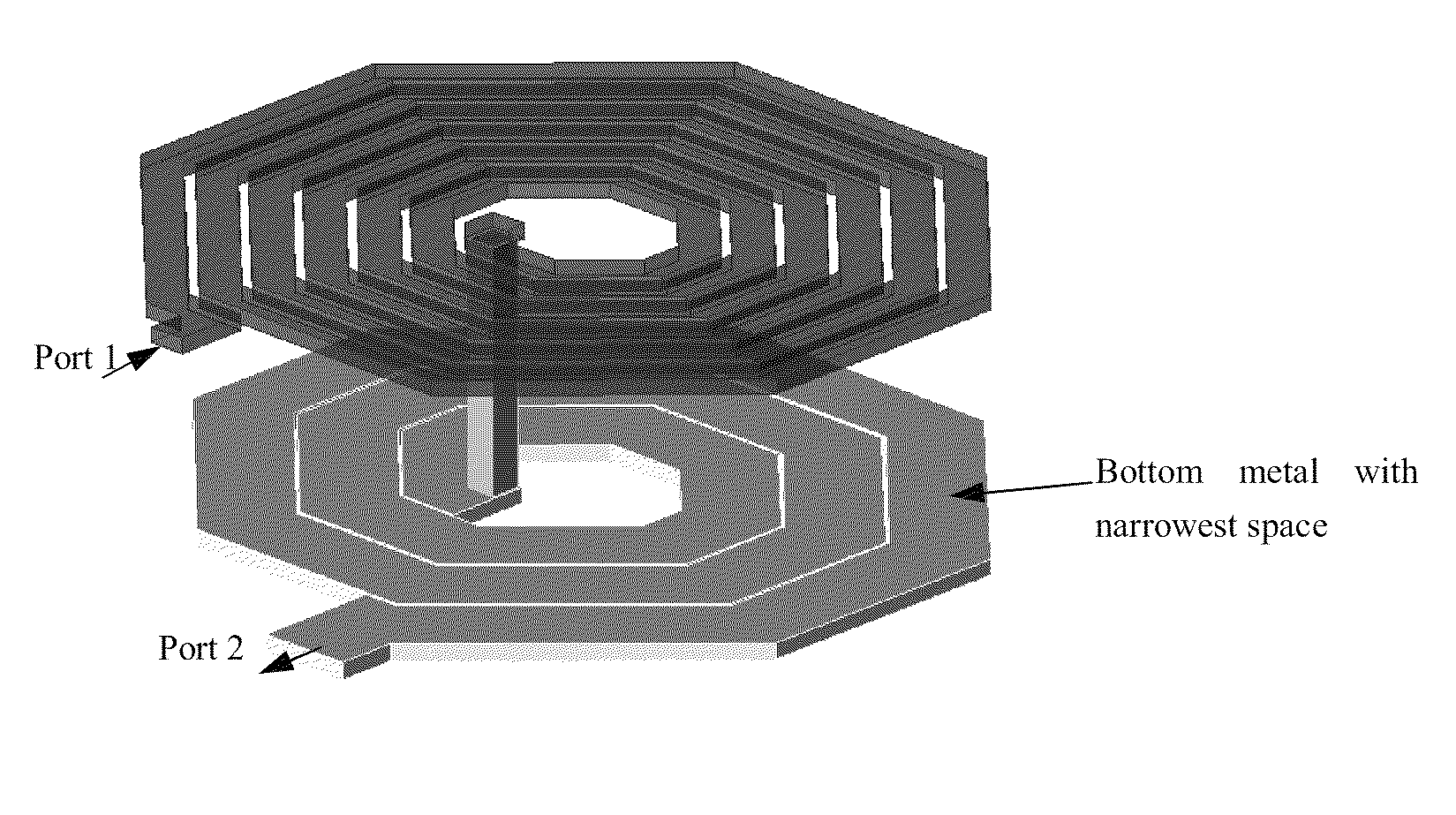
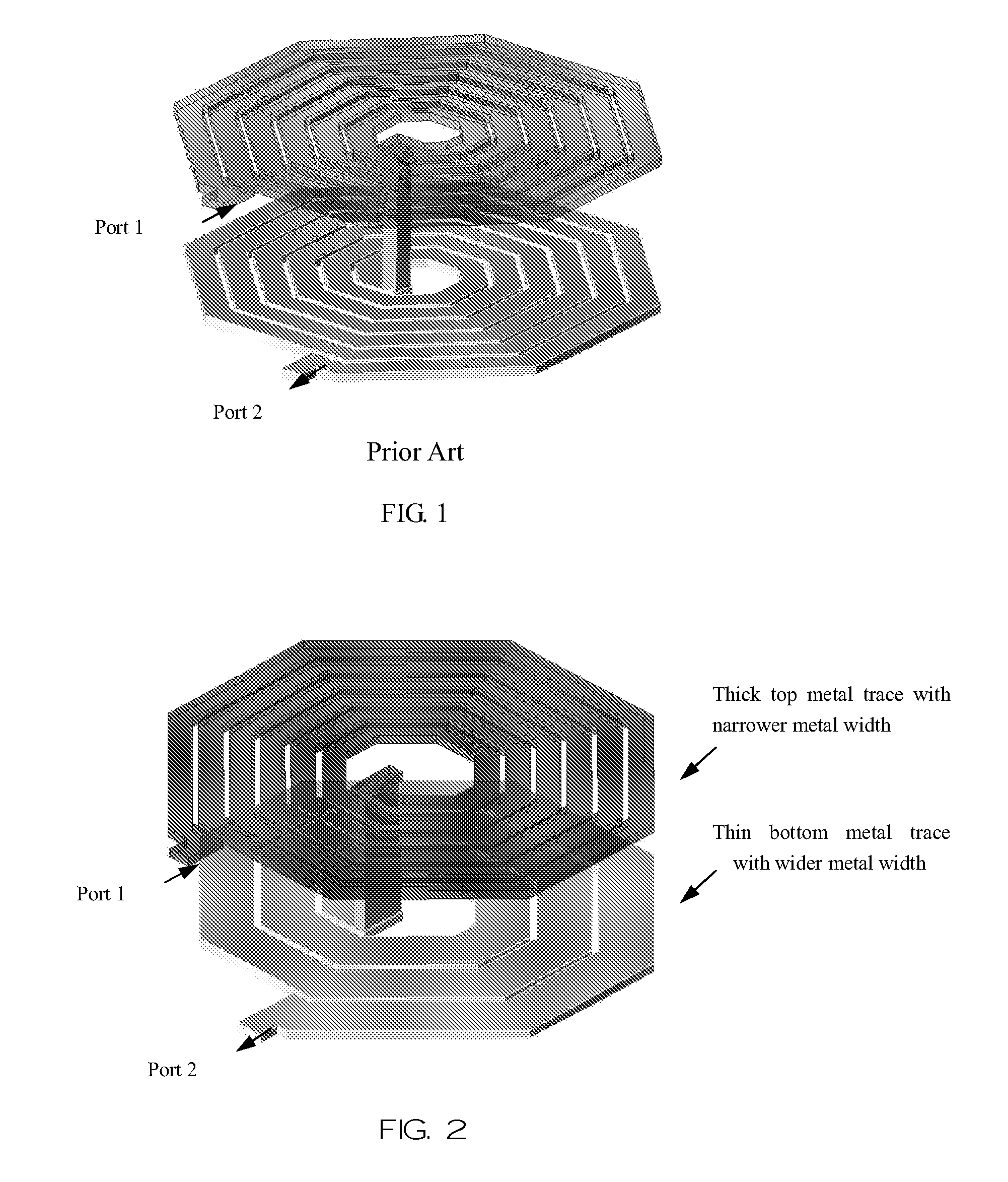
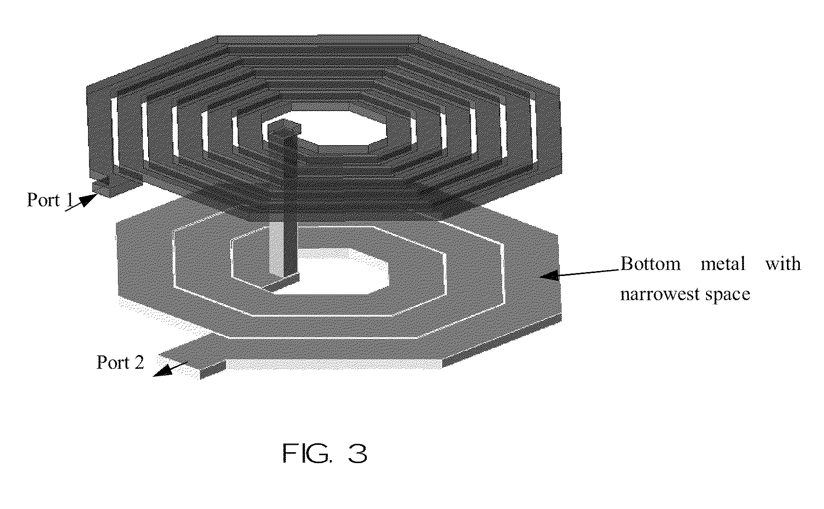
[0018]This stacked inductor with different metal thickness and metal width consists of two or more metal layers, this structure includes: top and bottom metal trace, which is aligned with each other. The thickness and width of top and bottom metal trace are different. The top and bottom metal trace are connected at the end of metal trace with via holes.

[0019]To make things more detailed, the layout of stacked inductor with different metal thickness and metal width (take two layers, octagonal stacked inductor for example) are shown in FIG. 2. From schematic diagram in FIG. 2, the wid...


PUM

PropertyMeasurementUnit
thicknessaaaaaaaaaa
thicknessaaaaaaaaaa
thicknessaaaaaaaaaa

Abstract

A stacked inductor with different metal thickness and metal width. The stacked inductor comprises top and bottom metal traces which are aligned with each other. The thickness and width of the top and bottom metal traces are different. The top and bottom metal traces are connected at the end of metal trace with via holes. The inductance is increased with the use of the mutual inductance between top and bottom metal layers The parasitic resistor is reduced due to the difference of the top and bottom metal widths.

Description

[0001]The current invention claims a foreign priority to the China application number 200910201904.X filed on Dec. 8, 2009.FIELD OF THE INVENTION[0002]The invention relates to micro-electronics and more particularly to realizing high Q on-chip stacked inductor for RF application.BACKGROUND OF THE INVENTION[0003]In present, there are a lot of passive devices in the integrated circuits. One of the most important components in RF CMOS / BiCMOS integrated circuits is on-chip inductor. Inductor has great impact on the RF characteristic in common wireless products. The design and analysis for this component has been widely researched as a result. Nowadays, the high Q on-chip inductor has been widely used in voltage controlled oscillator, low noise amplifier and other RF building blocks. On-chip stacked inductor reduced chip area in a large extent, which reduced the production cost.[0004]Q factor is the major specification of inductor, high Q means low loss and high efficiency.[0005]In tradi...

Claims


Application Information

Patent Timeline
Patent Type & Authority Patents(United States)
IPC IPC(8): H01F5/00H01F27/28
CPCH01F17/0013H01L23/5227H01F2017/0073H01L2924/0002H01L2924/00
Inventor CHIU, TZUYINXU, XIANGMINGCAI, MIAO
Owner SHANGHAI HUAHONG GRACE SEMICON MFG CORP
Why Eureka
Try Eureka