Multi-path laminated inductor with inner path and outer path current compensation function

A technology of current compensation and laminated inductance, applied in the field of microelectronics, can solve the problems of reduced quality factor, inconsistent current density inside and outside the coil, etc., and achieve the effect of reducing influence, reducing skin effect and proximity effect, and high inductance quality factor

Inactive Publication Date: 2011-06-08
SHANGHAI HUA HONG NEC ELECTRONICS
View PDF0 Cites 12 Cited by
  • Summary
  • Abstract
  • Description
  • Claims
  • Application Information

AI Technical Summary

Problems solved by technology

However, the current flowing in the coil inside the multi-turn inductor will be affected by the magnetic field of the inductor, resulting in inconsistent current density inside and outside the coil, resulting in a decrease in quality factor, so it cannot well meet the needs of circuit design

Method used


Image

  • Multi-path laminated inductor with inner path and outer path current compensation function
  • Multi-path laminated inductor with inner path and outer path current compensation function
  • Multi-path laminated inductor with inner path and outer path current compensation function

Examples


Embodiment Construction

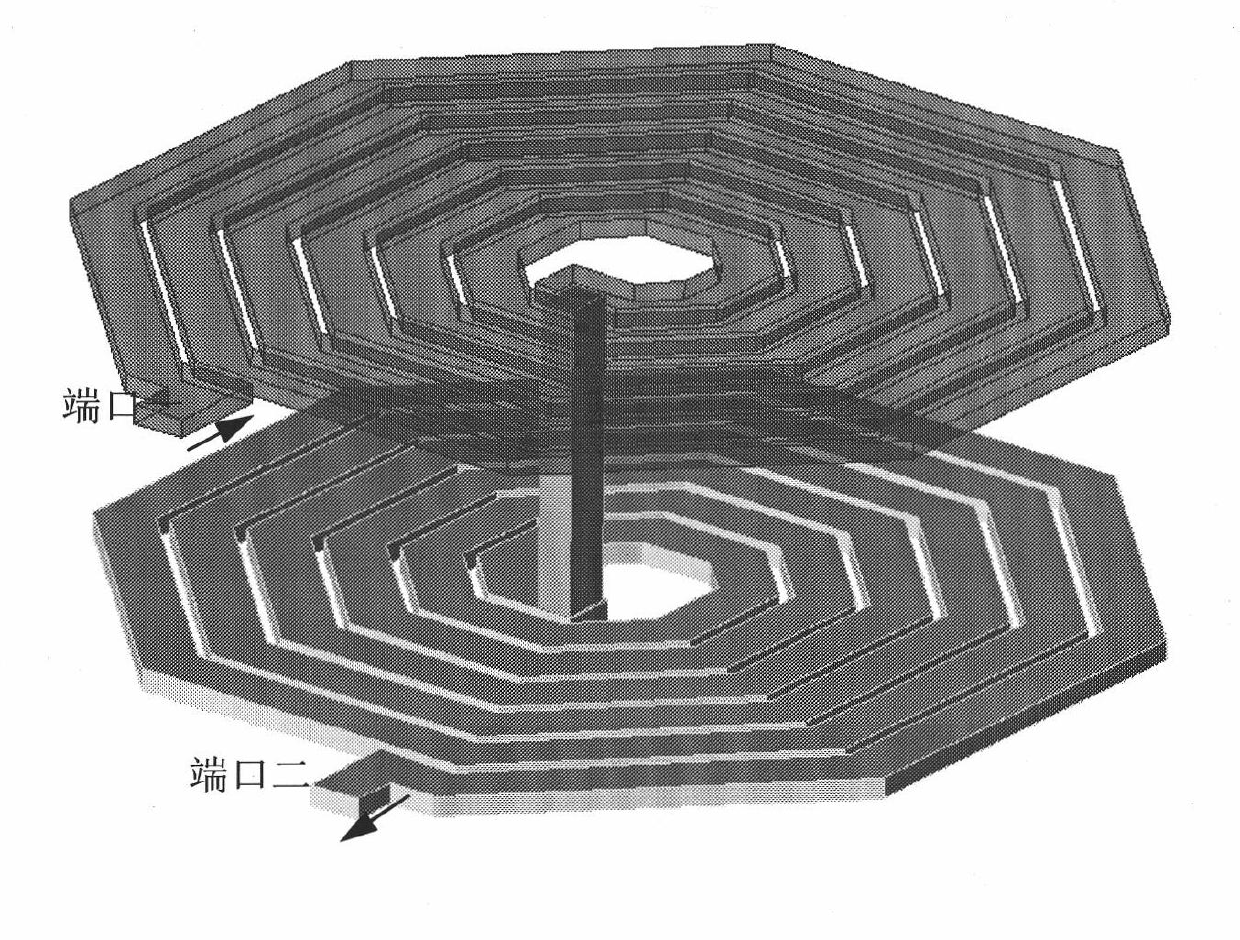
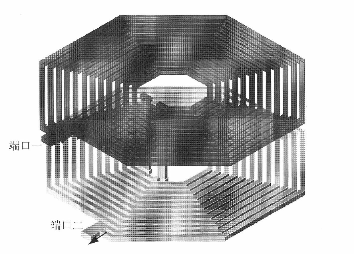
[0029] A multi-path laminated inductor with internal and external diameter current compensation according to the present invention; it is a multi-layer structure, including: upper and lower layer metal coils, the slotted parts of the upper and lower layer metal coil patterns overlap; the metal coil consists of multiple paths Composed of metal wires, the metal wires on the inner side of the first layer of metal coils are wound to the other layer of metal coils and turned over to connect to the outer side of the metal wires; the inner side of the other layer of metal coils is wound to the first layer of metal coils and turned over to connect The metal wires on the outer side are interconnected with the upper and lower metal coils.

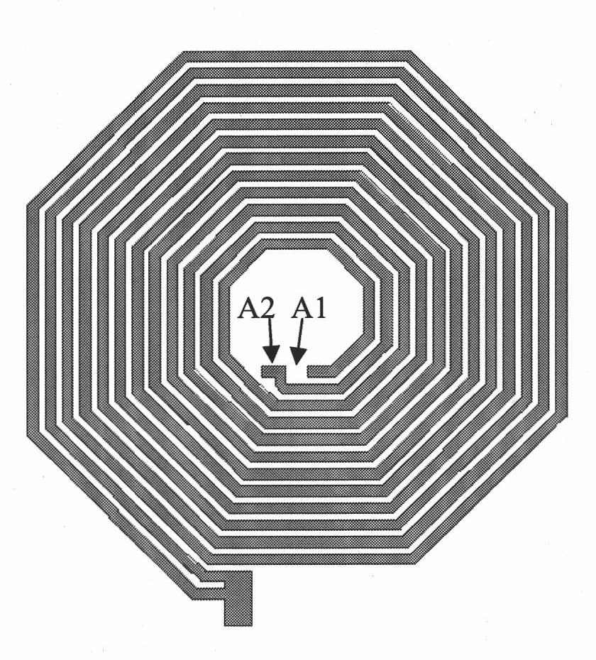
[0030] In more detail, the planar structure of stacked stacked inductors with upper and lower layers aligned in the present invention (taking two layers of metal and 6 turns of octagonal inductors as an example), its plan view is shown in image 3 , ...


PUM


Abstract

The invention discloses a multi-path laminated inductor with an inner path and outer path current compensation function. The multi-path laminated inductor has a multilayer structure and comprises an upper layer metal coil and a lower layer metal coil, wherein slotted parts of patterns of the upper layer metal coil and the lower layer metal coil are coincident with each other; each metal coil consists of a plurality of paths of metal wires; the path of metal wire inside the first layer of metal coil is wound to the other layer of metal coil, and is turned and connected to form an outer path of metal wire; the path of metal wire inside the other layer of metal coil is wound to the first layer of metal coil, and is turned and connected to form an outer path of metal wire; and the upper layer metal coil is interconnected with the lower layer metal coil. The invention provides a multi-coil laminated inductor with a new structure; and the influence of skin effect and proximity effect is reduced by dividing the plurality of paths and cross-connecting the upper layer metal and the lower layer metal. In the inductor, the inductance under the same area condition is improved to the great extent, and a higher inductance quality factor is effectively kept.

Description

technical field [0001] The invention relates to the field of microelectronics, in particular to a laminated inductor with a stacked structure. Background technique [0002] At present, a large number of passive devices are included in integrated circuits, among which on-chip inductors are a very important one, and on-chip inductors are one of the important components of radio frequency CMOS / BiCMOS integrated circuits. In typical wireless products, inductive components have a significant impact on the overall RF performance. Therefore, the design and analysis of these inductive components have also been extensively studied. As the core component of the RF circuit, the inductor can usually affect the overall performance of the entire circuit. At present, on-chip inductors with high quality factors are widely used in RF circuit modules such as voltage-controlled oscillators and low-noise amplifiers. The stacked on-chip inductor greatly reduces the chip area and reduces the p...

Claims


Application Information

Patent Timeline
Patent Type & Authority Applications(China)
IPC IPC(8): H01F17/00H01F37/00H01F27/28H01L23/522
CPCH01F2017/0053H01L23/5227H01F17/0013H01L2924/0002H01L2924/00
Inventor 邱慈云徐向明蔡描
Owner SHANGHAI HUA HONG NEC ELECTRONICS
Why Eureka
Try Eureka