Optical interconnect solution

a technology of optical interconnection and solution, applied in the direction of optical elements, circuit optical details, instruments, etc., can solve the problems of high resistance, large power consumption, high frequency electrical signals, etc., and achieve the effects of reliable microdevices, high speed connections, and low cos

Active Publication Date: 2011-03-08
II VI DELAWARE INC
View PDF29 Cites 11 Cited by
  • Summary
  • Abstract
  • Description
  • Claims
  • Application Information

AI Technical Summary

Benefits of technology

[0004]One advantage of the present invention is it permits high speed connections through a single (bare) fiber at a very low cost and very reliable microdevice. Another advantage of the invention is the capability of the connector in preventing connection failure due to improper seating of an optical fiber while simultaneously exhibiting a small footprint for easy incorporation into most PCB applications.
[0005]Accordingly, the present invention encompasses an optical connection between printed circuit boards, said connection being microsized so as to permit a single optical fiber to transfer optical signals converted from electrical impulses between said printed circuit boards. Furthermore, encompassed as well within the invention is such a micro-connection between printed circuit boards exhibiting a transfer rate of at least 10 Gb / s.
[0006]The present invention represents a significant improvement between the speed required for large memory-size transmissions and communications and the cost necessary to produce the information transfer component. Current electrical interconnects on printed circuit boards (“PCBs”) rely on electrical impulses to carry communication signals. As the speed of communication increases, however, the high frequency of the signals being transmitted via these electrical conductors increases as well and the skin effect principle begins to limit and degrade the ability to effectively transmit these signals. The skin effect effectively increases the resistance of the conductor to a point of limiting the communication possible via a particular pathway. As a solution, traditional electrical interconnects may be replaced with current optical technology but this solution is prohibitively expensive and impractical using current technology.
[0007]In order to solve the limitations in high speed communications, the current invention describes a low-cost optical interconnect solution. As a part of that solution, the current invention provides for the use of optical micro-connectors to couple bare optical fiber as a means of providing a communication pathway. An optical transmitter located on a PCB utilizes silicon circuitry to convert electrical impulses to optical signals. This signal is subsequently transmitted via the attached optical fiber to an end point where a receiving module converts the optical signal back to electrical impulses for transmission to related components on the PCB. The optical transmission of the signal eliminates the skin effect found in electrical transmissions and provides a much higher capacity link between components.
[0008]The above-described advantages are achieved by mounting an optical transmitter module and an optical receiver module directly onto a PCB with silicon circuitry near or underneath the module. These transmitting and receiving modules execute spatial optical transmission and reception of signals converted to and from electrical impulses by the silicon circuitry to which they are attached. Optical signals are transmitted between the optical transmitting module and the optical receiving module via an optical fiber held in position by an appropriate micro-connector.
[0009]More specifically, in one potentially preferred embodiment of the optical interconnection system, there is provided an optical connector for connecting electronic components co-located on the same PCB or on separate PCBs and having a first connector and second connector for transmitting and receiving information between such components. The first connector includes at least an optical transmitter that converts electric signal input to an optical signal output and transmits said data via an optical fiber to a second connector. The second connector includes at least one optical receiver module that converts optical signal input transmitted via an optical fiber from the optical transmitter module of the first connector and outputs an electrical signal output to be used by components on the PCB.

Problems solved by technology

As processing speeds increase, however, the skin effect of high frequency electrical signals can create a host of problems including high resistance, large power consumption, and a limited signal transmission distance.
While optical connections have always been known for their speed and reliability they have also been associated with a high cost of implementation.

Method used


Image

  • Optical interconnect solution
  • Optical interconnect solution

Examples


Embodiment Construction

[0018]Detailed embodiments of the present invention are disclosed herein; however, as will be readily apparent to those skilled in the art, the present invention may be produced in other specific forms without departing from its spirit or essential characteristics. The present embodiments, are therefore, to be considered as illustrative and not restrictive, the scope of the invention being indicated by the claims rather than the following description, and all changes which come within the meaning and range of the equivalence of the claims are therefore intended to be embraced therein.

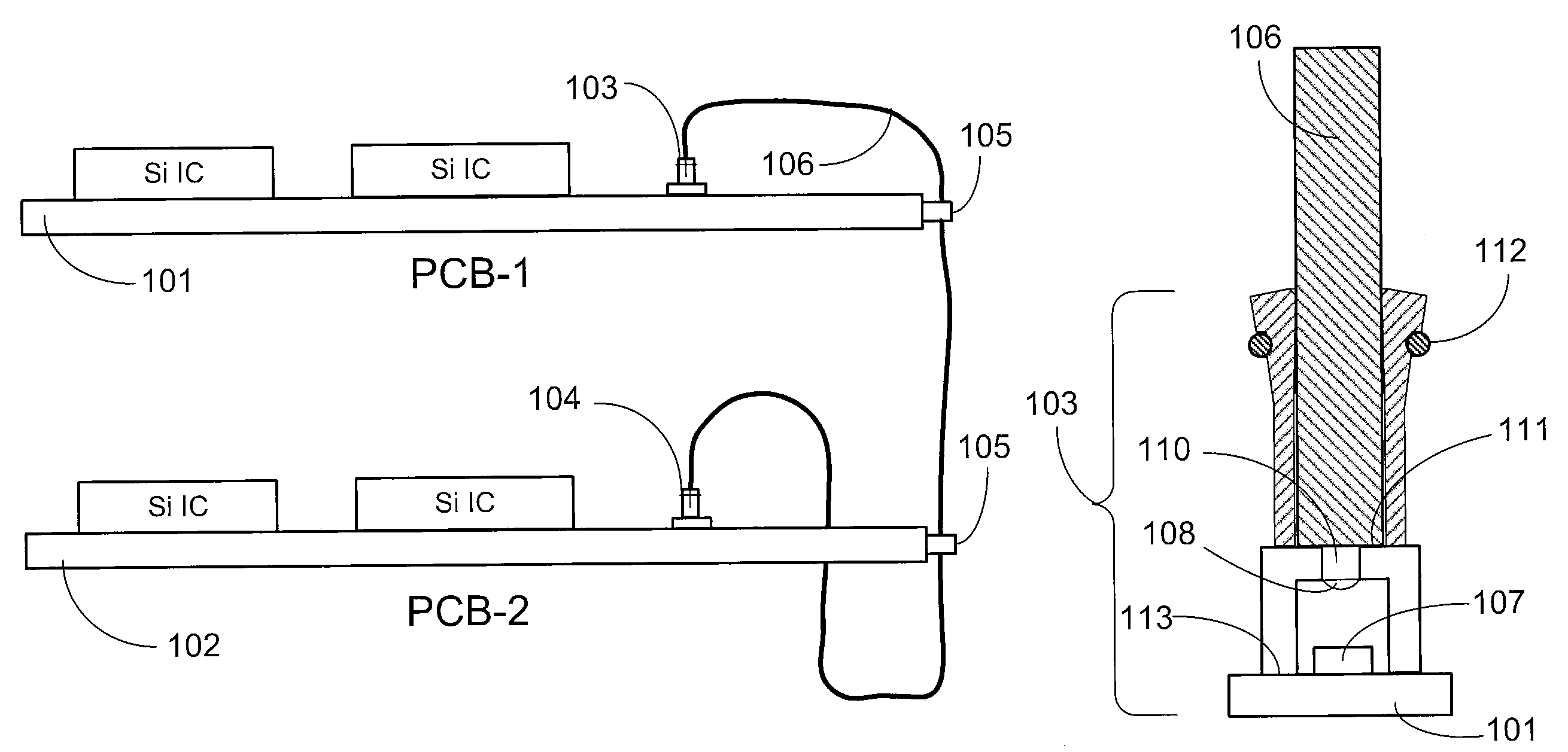
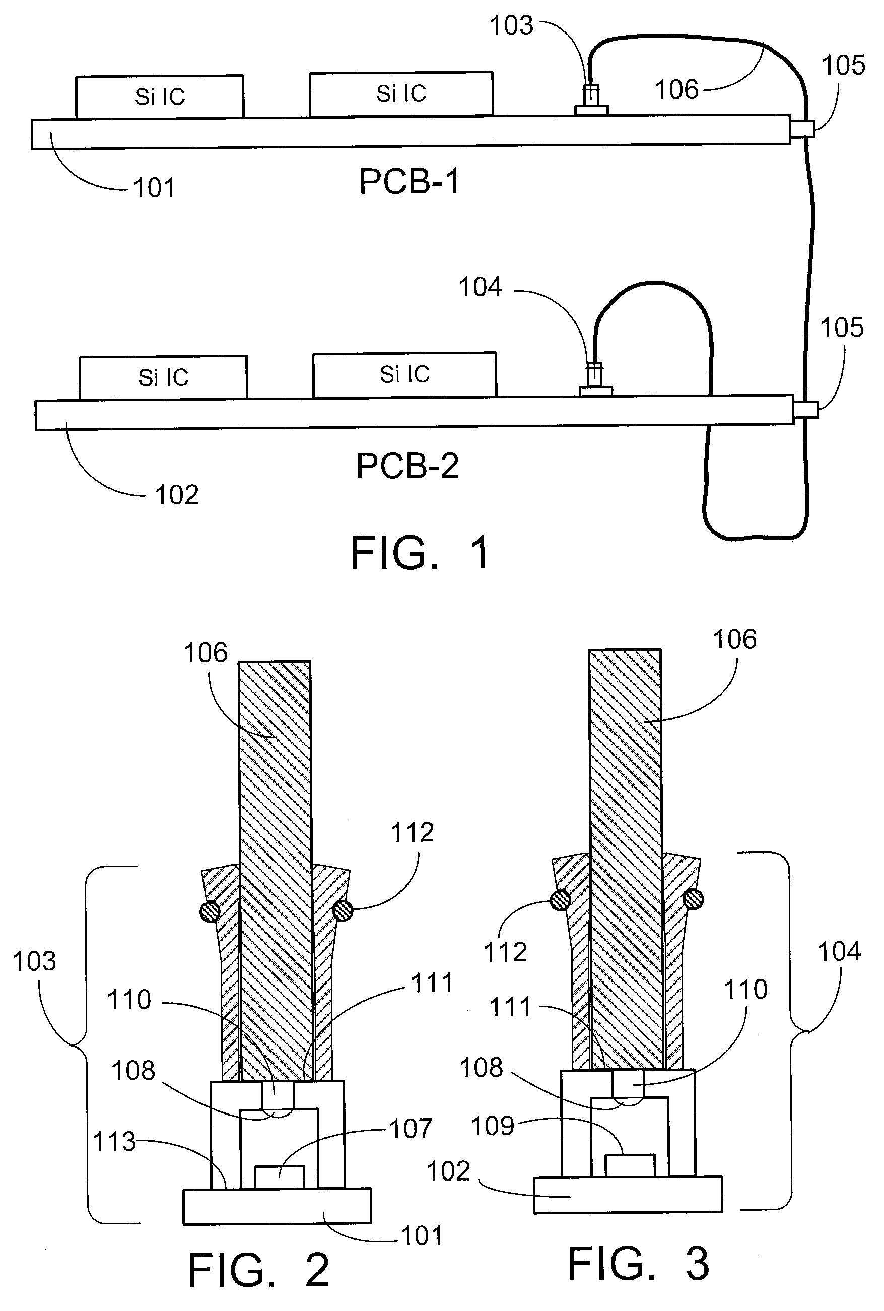
[0019]Referring to FIG. 1, a first connector 103 is attached to an originating PCB 101 and so integrated as to receive electrical signals to be transmitted to a receiving PCB 102. The electrical signals are converted by the first connector 103 to optical signals which are then transmitted via a bare optical fiber 106 (no ferrule or other type of cap or connector device is present or necessary). The bare...


PUM


Abstract

A low-cost, high-speed optical interconnect replacement for current electrical interconnects on printed circuit boards is provided. The invention achieves its goal by including an optical transmitter module or optical receiver module mounted in close proximity to a modulator used to encode optical signals from electrical impulses or decode optical signals to electrical impulses. A bare optical fiber is then used to transmit the signal from an optical encoding source to an optical receiver, providing a high-speed method of replacement for traditional electrical interconnects.

Description

FIELD OF THE INVENTION[0001]The present invention relates to a method for optical interconnection of electrical components in order to transmit data at a faster and more efficient rate of speed. The invention achieves its goal by including an optical transmitter module or optical receiver module mounted in close proximity to a modulator used to encode optical signals from electrical impulses or decode optical signals to electrical impulses. An optical fiber is then used to transmit the signal from an optical encoding source to an optical receiver, providing a high-speed method of replacement for traditional electrical interconnects.BACKGROUND OF THE INVENTION[0002]As future high speed computing technologies find a need to transfer large amounts of data from point to point within an electronic component, technologies will have to adapt in order to satisfy this requirement. The common solution today is to carry inter-circuit and intra-circuit signals via traditional electrical conduct...

Claims


Application Information

Patent Timeline
Patent Type & Authority Patents(United States)
IPC IPC(8): G02B6/42
CPCH04B10/801H05K1/144H05K1/0274H05K2201/042
Inventor DENG, HONGYU
Owner II VI DELAWARE INC
Why Eureka
Try Eureka