
Method for forming non-load-effect large size groove

A large-scale, no-load technology, used in electrical components, semiconductor/solid-state device manufacturing, circuits, etc., can solve the problems of fast etching speed, slow etching rate, and connection failure in small-scale trenches, and achieve improved etching. Process performance, the effect of expanding the etching process window, and improving product yield

Active Publication Date: 2012-11-14
SHANGHAI HUALI MICROELECTRONICS CORP
View PDF6 Cites 12 Cited by
  • Summary
  • Abstract
  • Description
  • Claims
  • Application Information

AI Technical Summary

Problems solved by technology

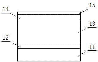
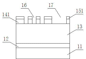
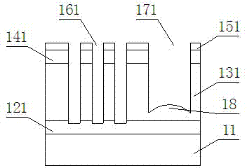
[0004] However, the single damascene trench etching process will produce a loading effect, which is mainly reflected in two aspects: first, when etching a silicon oxide trench, a large The concentration of etchant in the small-sized etching area (such as groove 17) is lower than that of the small-sized etching area (such as groove 16), the etching rate is slow, and the larger the difference in size, the more prominent the difference; Second, when etching silicon oxide trenches, due to the use of low fluorine-to-carbon ratio gases that generate more polymers to ensure the etching sidewall morphology, such as C4F8, C4F6 and other gases will cause more intense etching reactions in large-sized etching areas, resulting in more polymers and lower etching rates. Slow, coupled with ion reflection at the edge of the large-scale etched area, resulting in the formation of a large-scale etched area with a high middle and low etching profile on both sides
Under the combined effect of these two effects, the small-sized trench has the fastest etching rate, the large-sized trench has the second largest etching rate on both sides, and the middle etching rate is the slowest. The greater the size difference, the greater the etching rate difference. more obvious and difficult to overcome
In order to ensure that the ILD loss of small-sized trenches is not too large, it is necessary to control the over-etching time. In order to ensure that the middle silicon nitride of large-sized trenches can be etched clean, the over-etching time must be sufficient. If the etch rate of the trenches differs too much, the debugging window of this process will be very small. In extreme cases, silicon nitride residues in the middle of large-sized trenches will result, which will cause connection failure.
[0005] such as As shown in Figure 3 , after the main etching process, the bottom of the formed small-sized via hole 161 has been partially etched into the remaining silicon nitride (SiN) layer 121, while the large-sized via hole 171 The bottom is also located in the residual FSG layer 131, and forms a raised residual FSG 18 in the middle; such as Figure 4, after continuing the over-etching process, although the bottom of the formed large-size through hole 172 is partially etched to the remaining silicon nitride (SiN) layer 122, there are still residual FSG 181, at this time, the bottom of the formed small-sized via hole 162 has been etched into the relatively deep remaining silicon nitride (SiN) layer 122; for example, Figure 5, after the etching process of the etching barrier layer is performed finally, the formed small-sized via hole 163 is located in the remaining interlayer Dielectric layer 111, and silicon nitride 19 remains at the bottom of the large-sized through hole 173, which causes connection failure and reduces product yield

Method used


Image

  • Method for forming non-load-effect large size groove
  • Method for forming non-load-effect large size groove
  • Method for forming non-load-effect large size groove

Examples


Embodiment Construction

[0027] The specific embodiment of the present invention will be further described below in conjunction with accompanying drawing:

[0028] Figure 6-12 It is a schematic structural diagram of the process flow of the method for forming a large-size groove without load effect in the present invention;

[0029] like Figure 6-12 As shown, first, an interlayer dielectric layer (inter layer dielectric, ILD for short) 21 with a thickness of 300A, a barrier layer 22 made of SiN with a thickness of 2500A, and a barrier layer 22 made of SiN with a thickness of 400A are sequentially deposited from bottom to top on the semiconductor structure 2 . A low dielectric constant dielectric layer 23 of silicon oxide (FSG) containing F, a metal hard mask 24 made of TiN with a thickness of 50A, and a metal hard mask 24 made of silicon dioxide (SiO 2 ) oxide layer 25; wherein, the interlayer dielectric layer 21 covers the upper surface of the semiconductor structure 2, the barrier layer 22 covers...


PUM


Abstract

The invention relates to the field of semiconductor manufacture, in particular to a method for forming a non-load-effect large size groove. Large size and small size contact hole grooves are filled in a deposition medium layer after the metal hard mask etching process, the grinding process is utilized to form a dish recessed area on the large size grooves, load effect formed in etching of the grooves with large size difference is removed, and connection efficacy lose caused by residue caused by the load effect in the large size grooves is effectively avoided. The method improves product yield, further expands an etching process window and further improves etching process performance.

Description

technical field [0001] The invention relates to the field of semiconductor manufacturing, in particular to a method for forming a large-size trench without load effect. Background technique [0002] Metal hard mask single damascene trench etching process is a key step in the copper wire interconnection process in the back section of the chip. After the etched trench is filled and polished with copper, the first layer of copper wire is formed, and the contact with the lower layer The contacts are connected, and the etching body is generally low dielectric constant silicon oxide or F-containing silicon oxide (FSG) film. [0003] Figure 1-5 It is a schematic diagram of the process flow structure of metal hard mask single damascene trench etching in the background technology of the present invention; as Figure 1-5 As shown, in the single damascene trench etching process of silicon oxide film containing F, silicon nitride (SiN) layer 12, FSG Layer 13, metal hard mask layer (Ti...

Claims


Application Information

Patent Timeline
IPC IPC(8): H01L21/768
Inventor 杨渝书李程陈玉文
Owner SHANGHAI HUALI MICROELECTRONICS CORP
Learn More