Methods of making stackable wiring board having electronic component in dielectric recess

a technology of dielectric recess and electronic component, which is applied in the direction of printed circuit aspects, semiconductor/solid-state device details, printed element electric connection formation, etc., can solve the problems of low manufacturing yield, device failure, and extreme difficulty in placing electronic devices at pre-designated locations

Inactive Publication Date: 2017-02-02
BRIDGE SEMICON
View PDF4 Cites 14 Cited by
  • Summary
  • Abstract
  • Description
  • Claims
  • Application Information

AI Technical Summary

Benefits of technology

[0011]The methods of making a stackable wiring board according to the present invention have numerous advantages. For instance, inserting the electronic component into the recess of the dielectric base is particularly advantageous as the minimal height of the metal posts needed for the vertical connection between the dual buildup circuitries at both opposite sides of the electronic component can be reduced by an amount equal to the depth of the recess. Additionally, the recess can ensure the placement accuracy of the electronic component to avoid micro-via connection failure in the subsequent formation of the buildup circuitries.

Problems solved by technology

However, it is extremely difficult to place an electronic device at a pre-designated location with micron-scale accuracy if the device is attached to a dielectric layer by an adhesive as described in U.S. Pat. Nos. 8,536,715 and 8,501,544.
A minor dislocation of the device due to adhesive curing or poor binding strength may lead to I / O disconnection, device failure and low manufacturing yield.
However, as the protruded bump of the embedded device causes undesirable increase in board thickness, the soldering approach usually does not meet stringent requirements for portables.

Method used


Image

  • Methods of making stackable wiring board having electronic component in dielectric recess
  • Methods of making stackable wiring board having electronic component in dielectric recess
  • Methods of making stackable wiring board having electronic component in dielectric recess

Examples


embodiment 1

[0069]FIGS. 1-15 are schematic views showing a method of making a wiring board that includes a dielectric base, metal posts, a stiffener, an electronic component and dual buildup circuitries in accordance with the first embodiment of the present invention.

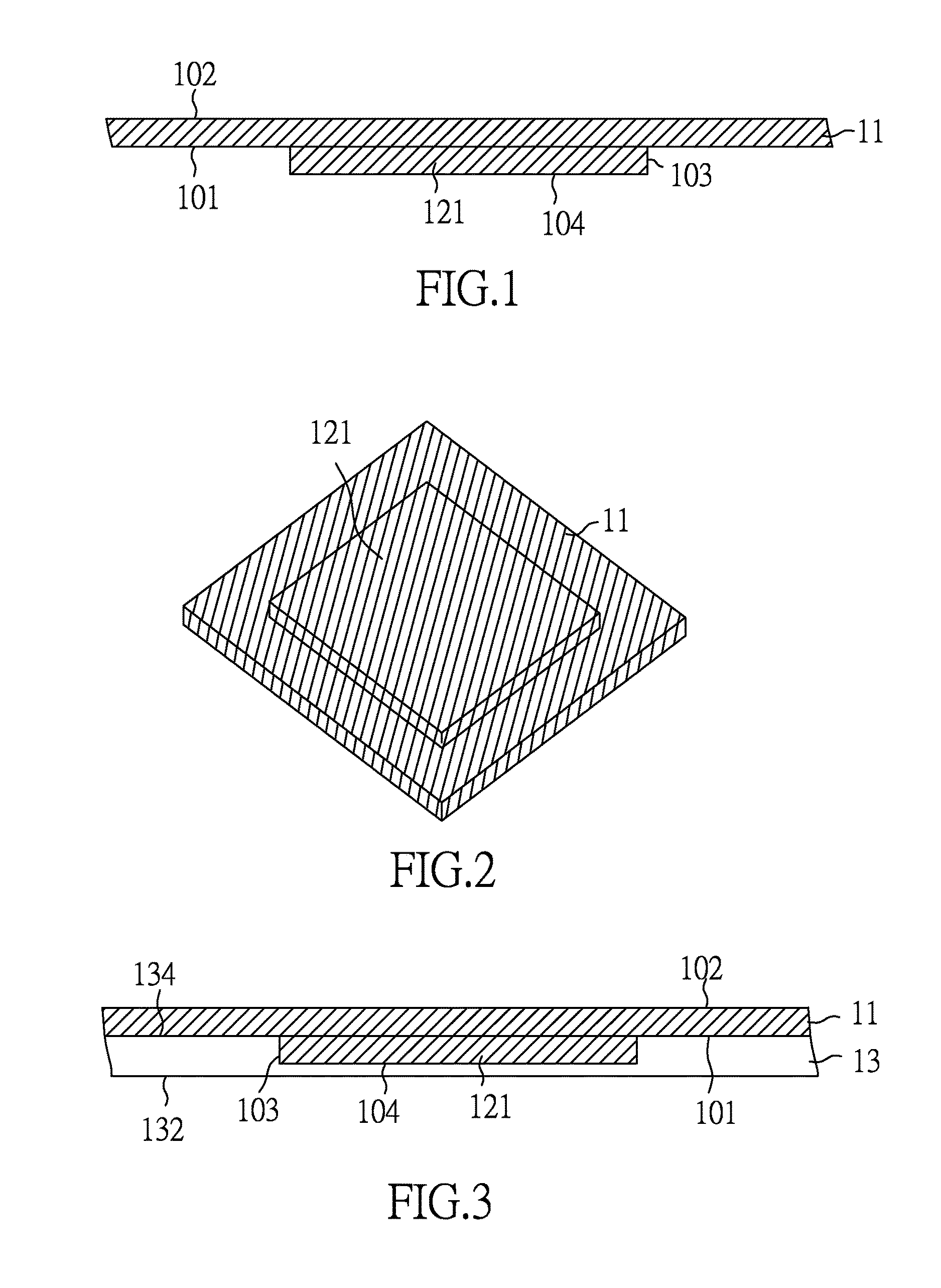
[0070]FIGS. 1 and 2 are cross-sectional and bottom perspective views, respectively, of the structure with a protruded metal platform 121 formed on a metal carrier 11. The metal carrier 11 and the protruded metal platform 121 typically are made of copper, aluminum, nickel or other metals or alloys. The material of the protruded metal platform 121 may be the same as or different from that of the metal carrier 11. The thickness of the metal carrier 11 can range from 0.05 to 0.5 mm (preferably from 0.1 to 0.2 mm), whereas the thickness of the protruded metal platform 121 can range from 10 to 100 microns. In this embodiment, the metal carrier 11 is made of copper and has a thickness of 0.125 mm, whereas the protruded metal platform 121 ...

embodiment 2

[0087]FIGS. 17-22 are schematic views showing a method of making a wiring board with the second buildup circuitry thermally conductible to the electronic component in accordance with the second embodiment of the present invention.

[0088]For purposes of brevity, any description in Embodiment 1 above is incorporated herein insofar as the same is applicable, and the same description need not be repeated.

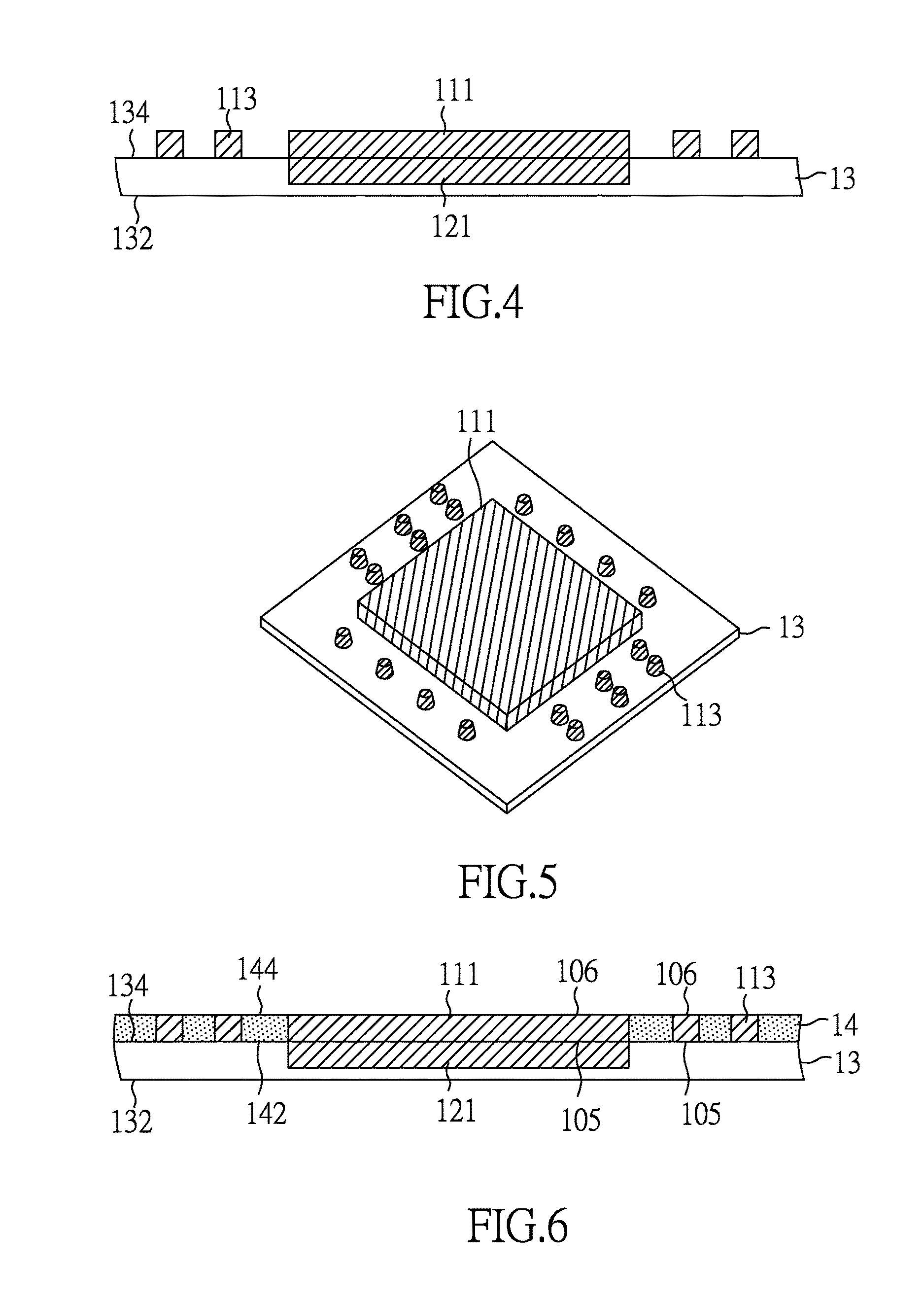
[0089]FIGS. 17 and 18 are cross-sectional and top perspective views, respectively, of the structure with metal posts 113 on a dielectric base 13. The structure is similar to that illustrated in FIG. 7, except that no stiffener is provided in this embodiment.

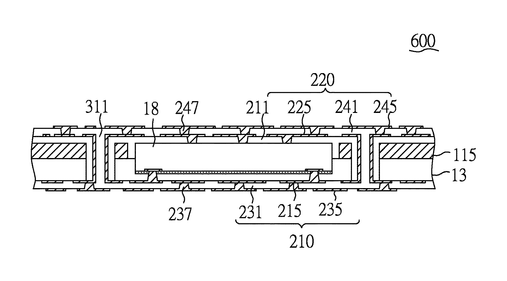
[0090]FIG. 19 is a cross-sectional view of the structure with an electronic component 18 placed in the recess 130 of the dielectric base 13. The electronic component 18 is inserted into the recess 130 and attached to the floor 136 of the recess 130 by an adhesive 16. In this embodiment, the electronic component 18 is illustrated as a ...

embodiment 3

[0098]FIGS. 24-34 are schematic views showing a method of making a wiring board with a metal layer deposited in the recess in accordance with the third embodiment of the present invention.

[0099]For purposes of brevity, any description in the aforementioned Embodiments is incorporated herein insofar as the same is applicable, and the same description need not be repeated.

[0100]FIG. 24 is a cross-sectional view of the structure with a protruded metal platform 121 and an array of auxiliary metal pads 123 formed on a metal carrier 11. The protruded metal platform 121 and the auxiliary metal pads 123 extend from the first surface 101 of the metal carrier 11 in the downward direction. In this illustration, each of the auxiliary metal pads 123 is substantially coplanar with the protruded metal platform 121 at its first and second surfaces 107, 108. The auxiliary metal pads 123 can be made of the same material as the protruded metal platform 121, and may be formed by pattern deposition, suc...


PUM


Abstract

A method of making a stackable wiring board is characterized by positioning an electronic component in a dielectric recess to realize the thickness reduction of the wiring board and sidewalls of the recess can confine the dislocation of the electronic component to avoid misalignment between buildup circuitry and the electronic component. An array of metal posts that provide vertical electrical connections are formed by using the same metal carrier that forms the recess, so that the predetermined distance and relative location between metal posts and pads/bumps of the electronic component can be maintained.

Description

CROSS REFERENCE TO RELATED APPLICATIONS[0001]This application claims the benefit of filing date of U.S. Provisional Application Ser. No. 62 / 198,058 filed Jul. 28, 2015. The entirety of said Provisional application is incorporated herein by reference.FIELD OF THE INVENTION[0002]The present invention relates to methods of making a wiring board, more particularly, to a method of making a stackable wiring board having an electronic component confined in a recess of a dielectric base and the component-in-recess is surrounded by an array of metal posts or plated through holes that provide vertical connection for the board.DESCRIPTION OF RELATED ART[0003]Market trends of multimedia devices demand for faster and slimmer designs. One of the approaches is to embed an electronic device in a wiring board so that the electrical performance of the board can be improved and / or another device(s) can be assembled on the board to form a 3D stacking structure. U.S. Pat. Nos. 8,193,034, 8,354,746, 8,38...

Claims


Application Information

Patent Timeline
Patent Type & Authority Applications(United States)
IPC IPC(8): H05K3/32H05K3/46H05K3/40
CPCH05K3/32H05K3/46H05K3/4015H05K3/4038H01L23/5389H01L24/19H01L24/73H05K1/185H05K3/4605H05K3/4647H05K3/4679H05K3/4697H05K2201/09036H05K2201/096H05K2203/167H05K2203/308H01L2224/04105H01L2224/92144H01L2924/15153H01L2224/2518H01L2224/32225H01L2224/73267H01L2224/92244H01L2224/32245H01L2924/3511H01L2224/18
Inventor LIN, CHARLES W. C.WANG, CHIA-CHUNG
Owner BRIDGE SEMICON
Why Eureka
Try Eureka