Packaging layer and packaging device

A technology for encapsulating devices and encapsulating layers, which is applied in the direction of electric solid-state devices, semiconductor devices, organic semiconductor devices, etc., can solve the problems of poor effect, fragile encapsulating layer structure, low optical coupling output rate, etc., and achieve good fluidity and improve Optical coupling output, the effect of improving stability

Inactive Publication Date: 2017-02-15
WUHAN CHINA STAR OPTOELECTRONICS TECH CO LTD
View PDF4 Cites 24 Cited by
  • Summary
  • Abstract
  • Description
  • Claims
  • Application Information

AI Technical Summary

Problems solved by technology

Although researchers have tried to increase light extraction by adding micro-refraction or diffraction structures (micro-lenses, scattering layers, etc.), the results are not good, such as the structure of the packaging layer is relatively fragile, the light coupling output rate low level problem

Method used


Image

  • Packaging layer and packaging device
  • Packaging layer and packaging device
  • Packaging layer and packaging device

Examples


Embodiment Construction

[0017] The present invention will be described in detail below in conjunction with the accompanying drawings and embodiments.

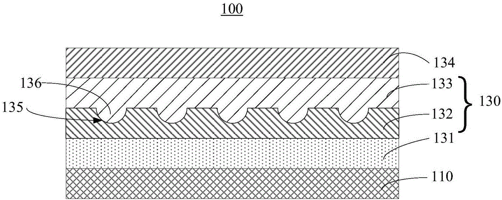
[0018] see figure 1 , the present invention provides a packaging device 100, the packaging device 100 can be but not limited to organic light emitting diodes, photoelectric testers, biosensors, solar cells, electronic paper, smart labels and the like. In this embodiment, the packaging device 100 is described by taking an organic light emitting diode as an example. The packaging device 100 includes a substrate to be packaged 110 and a packaging layer 130 , and the packaging layer 130 includes a base layer 131 , a first inorganic functional layer 132 , an organic buffer layer 133 and a second inorganic functional layer 134 .

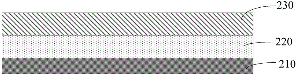
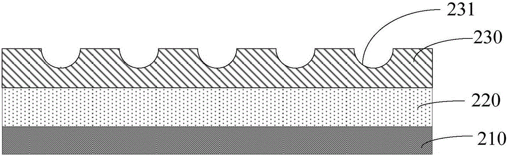
[0019] The base layer 131 is in contact with the substrate to be packaged (not shown), and the material of the base layer 131 is polyimide.

[0020] The first inorganic functional layer 132 covers the surface of the base layer 1...


PUM


Abstract

The invention provides a packaging layer comprising a first inorganic functional layer and an organic buffer layer covering the first inorganic functional layer. A plurality of grooves are formed in the surface, in contact with the organic buffer layer, of the first inorganic functional layer and a plurality of protrusions corresponding to and matching the multiple grooves are arranged on the surface, in contact with the first inorganic functional layer, of the organic buffer layer, so that the multiple protrusions can be embedded into the corresponding multiple grooves respectively. In addition, the invention also provides a packaging device. According to the packaging layer, the optical coupling output of the packaging device can be improved effectively. Moreover, bending, folding, and even rolling of the packaging device can be realized, so that stability of the packaging device is improved and thus the service life of the packaging device is prolonged.

Description

technical field [0001] The present invention relates to the technical field of display panels, in particular to an encapsulation layer and an encapsulation device. Background technique [0002] Organic Light Emitting Diode (OLED) is a new display and lighting technology, which not only can realize high-resolution or high-resolution display, but also shows great market potential in the field of large-area lighting and flexible display. In recent years, through continuous optimization and upgrading of materials and devices, OLEDs can achieve photoelectric conversion with an internal quantum efficiency of 100%. However, in an OLED device, light from the light-emitting layer to the outside will pass through organic layers, functional layers, and substrates with a higher refractive index than air, so only about 30% of the light is actually emitted to the outside. Although researchers have tried to increase light extraction by adding micro-refraction or diffraction structures (mi...

Claims


Application Information

Patent Timeline
Patent Type & Authority Applications(China)
IPC IPC(8): H01L51/52
CPCH10K50/85H10K50/844H10K2102/311
Inventor 金江江徐湘伦黄金昌蒋谦
Owner WUHAN CHINA STAR OPTOELECTRONICS TECH CO LTD
Why Eureka
Try Eureka