Optical element damage detecting device and method based on polarization imaging

A technology for optical components and damage detection, which is used in measurement devices, optical testing of flaws/defects, and material analysis by optical means. Effect

Inactive Publication Date: 2017-02-22
THE 41ST INST OF CHINA ELECTRONICS TECH GRP
View PDF4 Cites 14 Cited by
  • Summary
  • Abstract
  • Description
  • Claims
  • Application Information

AI Technical Summary

Problems solved by technology

[0004] At present, dark field imaging technology is mainly used for detection, but dark field imaging technology also has limitations, such as low edge positioning accuracy and loss of large-scale damage information. In addition, the total internal reflection illumination method can only be applied to flat panels. Inspection of Optical Components

Method used


Image

  • Optical element damage detecting device and method based on polarization imaging
  • Optical element damage detecting device and method based on polarization imaging

Examples


Embodiment 1

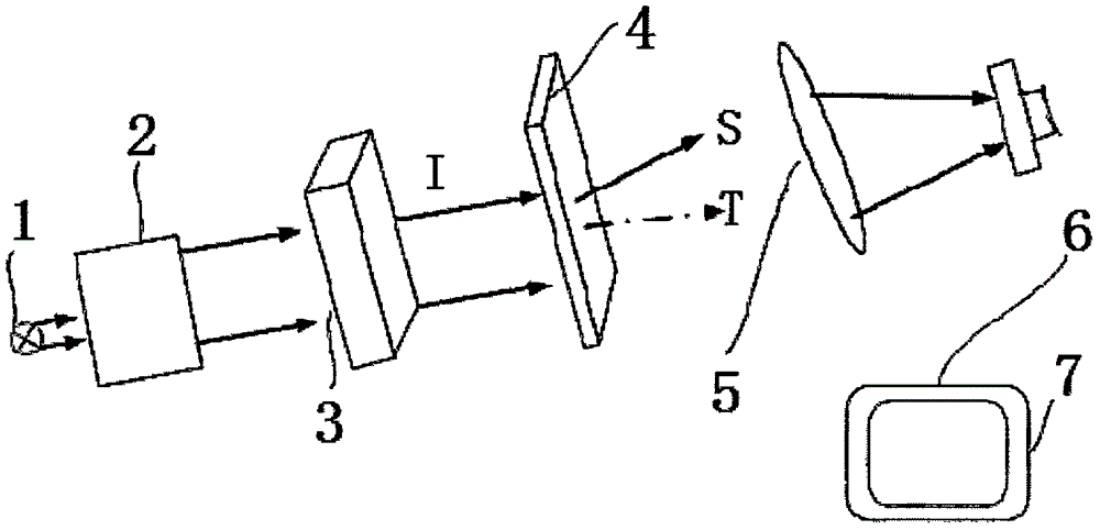
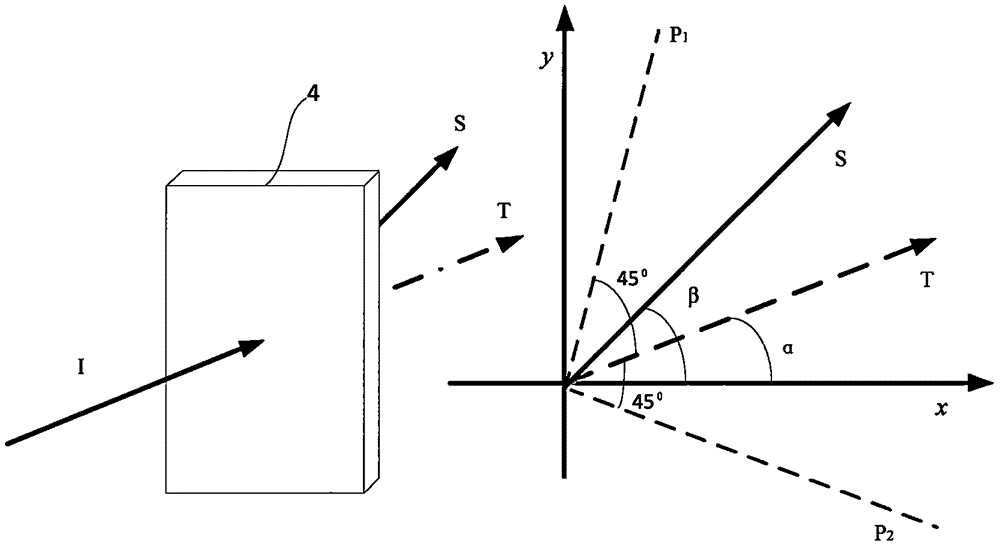
[0037] An optical element damage detection device based on polarization imaging proposed by the present invention includes a light source 1 and a beam expander system 2 arranged sequentially along the light source 1, a linear polarizer 3, an optical element under test 4, an imaging system 5, and a CCD Detector 6 , processing computer 7 , optical element under test 4 and CCD detector 6 are respectively located on the object plane and image plane of imaging system 5 , and the output end of CCD detector 6 is connected with the input end of processing computer 7 .

[0038] The beam expansion ratio of the beam expander system 2 is 5ט25×, and the maximum aperture is 300 mm.

[0039] The linear polarizer 3 adopts a quartz plate stack structure design, which is composed of 20 pieces of quartz flat glass, and the polarization degree of the outgoing light is better than 99%.

[0040] The imaging system 5 adopts a zoom design, the focal length range is 100mm-200mm, the field of view is ...

Embodiment 2

[0060] An optical element damage detection device based on polarization imaging proposed by the present invention includes a light source 1 and a beam expander system 2 arranged sequentially along the light source 1, a linear polarizer 3, an optical element under test 4, an imaging system 5, and a CCD Detector 6 , processing computer 7 , optical element under test 4 and CCD detector 6 are respectively located on the object plane and image plane of imaging system 5 , and the output end of CCD detector 6 is connected with the input end of processing computer 7 .

[0061] The beam expansion ratio of the beam expander system 2 is 10ט40×, and the maximum aperture is 500 mm.

[0062] The linear polarizer 3 adopts a quartz plate stack structure design, which is composed of 25 pieces of quartz flat glass, and the polarization degree of the outgoing light is better than 99%.

[0063] The imaging system 5 adopts a zoom design, the focal length ranges from 200mm to 400mm, the field of v...


PUM


Abstract

The invention relates to an optical element damage detecting device and method based on polarization imaging. The optical element damage detecting device comprises a light source as well as a light beam expanding system, a linear polarizer, a detected optical element, an imaging system, a CCD detector and a processing computer which are arranged sequentially along the light source, wherein the detected optical element and the CCD detector are located on an object plane and an image plane of the imaging system respectively, and an output end of the CCD detector is connected with an input end of the processing computer. According to the optical element damage detecting device and method based on polarization imaging, linearly polarized light is used for illuminating the optical element, the polarization CCD detector receives scattered light S and direct transmission light T of a damage point of the optical element, mutually orthogonal linear polarization images are obtained, the direct transmission light is filtered out by means of the difference of the orthogonal linear polarization images, images of the damage point of the optical element are enhanced, and the measurement problem that the optical element image detecting method cannot give consideration to image resolution, edge location accuracy, large-sized damage information and the like simultaneously is solved.

Description

technical field [0001] The invention relates to the field of optical element damage detection, in particular to a polarization imaging-based optical element damage detection device and method. Background technique [0002] The research and application technology of high-power lasers is one of the important research contents in the field of laser and laser application technology. It is one of the research frontiers in the field of laser optics in the world today. It has important application background and far-reaching scientific significance. Therefore, advanced countries in the world have invested a lot of manpower, material resources and financial resources in the research of strong laser technology. Among them, the transmission of high-power laser and the control of beam quality are of great interest and one of the main research contents of experts and scholars in the laser field from all over the world. When the high-power laser passes through the optical element, the p...

Claims


Application Information

Patent Timeline
Patent Type & Authority Applications(China)
IPC IPC(8): G01N21/88G01N21/95
CPCG01N21/8851G01N21/95G01N2021/8848
Inventor 赵发财孙权社王少水王国权郑祥亮韩忠
Owner THE 41ST INST OF CHINA ELECTRONICS TECH GRP
Why Eureka
Try Eureka