Inductor for integrated circuit

A circuit and device technology, applied in the structural field of making inductors, can solve problems such as complex inductance and non-constant inductance

Inactive Publication Date: 2002-06-12
IBM CORP
View PDF12 Cites 5 Cited by
  • Summary
  • Abstract
  • Description
  • Claims
  • Application Information

AI Technical Summary

Problems solved by technology

[0014] In summary, there are several problems with the prior art: making the inductor requires a particularly complex and expensive process, requires a high-resistivity substrate to reduce coupling to the inductor, and the inductance is not constant over a fairly wide frequency range

Method used


Image

  • Inductor for integrated circuit
  • Inductor for integrated circuit
  • Inductor for integrated circuit

Examples


Embodiment Construction

[0039] The microstrip transmission line of the present invention is adopted in the following several structures:

[0040] - Straight line microstrip

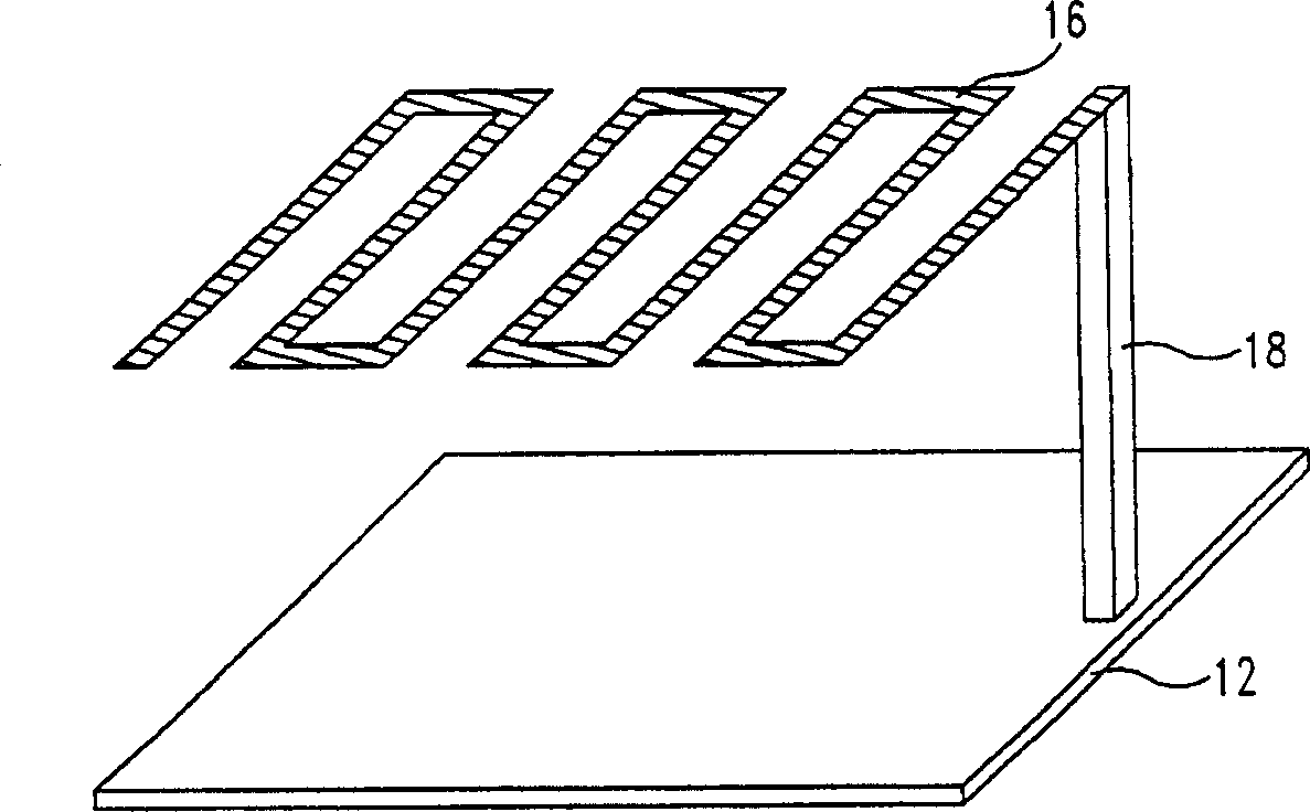
[0041] -Curve structure

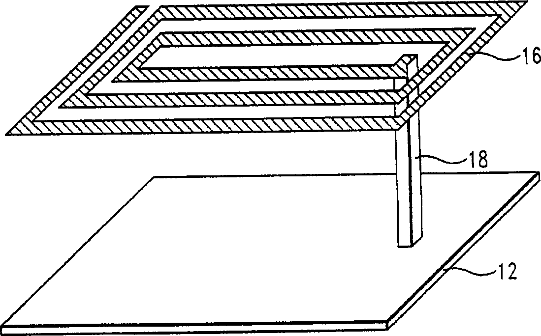
[0042] - helical structure

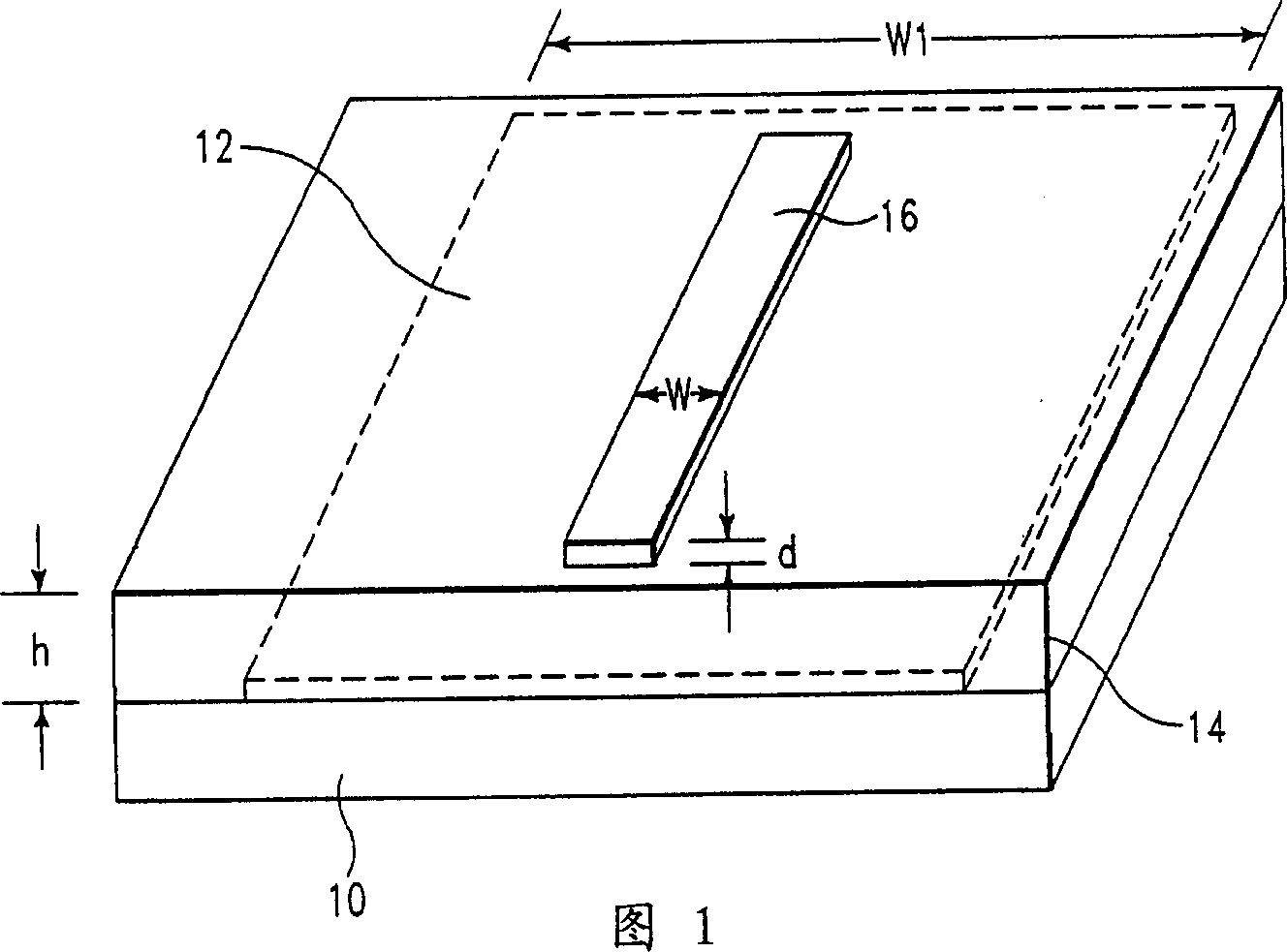
[0043]The linear microstrip structure is shown in FIG. 1, in which the center conductor 16 as a signal transmission conductor is made of aluminum or copper. The two types of metallization techniques have different advantages for system optimization. Copper has a lower resistivity than aluminum, but aluminum wire can be made thicker without special treatment. It is desirable to increase the thickness of the center conductor to achieve lower overall resistance. The width of the center conductor is W, the thickness is d, and the distance between the center conductor and the metal plane 10 below it is h, which is an interlayer insulating material in the integrated chip substrate 10 . The integrated chip substrate preferably contains a multifunctional integrated circuit to w...


PUM

PropertyMeasurementUnit
thicknessaaaaaaaaaa
thicknessaaaaaaaaaa
thicknessaaaaaaaaaa

Abstract

An inductor is integrated in VLSI and ULSI technology products for very high frequency applications. The inductor is in a microstrip transmission line configuration which can be designed in a form of straight line, spiral line or Meander line. The inductor is formed by shorting the microstrip center conductor to the lower level ground plane at one end of the transmission line. This results in an inductance which, for a given design of transmission line, and in a specified frequency range, is independent of frequency, within the operating design range. The microstrip transmission line provides an inductance which could be used on any type of substrate, with either low or high resistivity. The microstrip transmission line could utilize two or all of the metal wiring levels of the technology, allowing a wide range of inductance and quality factor design tradeoffs. An important feature in this trade-off is the ability to utilize lower (below the inductor) metal wiring levels, as well as lower silicon and polysilicon areas for other than inductor design purposes, without affecting the operation of the inductor. This is because of the isolation properties of this inductor system. By utilizing isolation layers with low relative dielectric constant, Further enhancements of the system are achieved. The inductance of this system is constant within 10% over a frequency range extending from about 8 GHz to about 35 GHz This inductor system allows the design to be optimized, through several parameters, to achieve the desired performance.

Description

technical field [0001] The present invention relates to the enhancement of inductors for use in integrated circuit technology, and more particularly to structures and methods for fabricating inductors which do not substantially disrupt conventional semiconductor fabrication techniques. Background technique [0002] Fabrication of on-chip inductors in combination with modern integrated circuits is highly desirable for many applications. [0003] A major disadvantage of integrated inductors, especially on low-resistivity substrates, is the significant electric and magnetic field coupling between the inductive element and the conductive substrate. First, this will reduce the resulting inductance since any induced current in the substrate will result in a magnetic field oriented opposite to that of the inductor (Lenz's law). This magnetic field opposing the inductor's field causes the overall field to weaken as frequency increases, producing a varying eff...

Claims


Application Information

Patent Timeline
Patent Type & Authority Applications(China)
IPC IPC(8): H01L23/522
CPCH01L2924/0002H01L2924/3011H01L23/5227H01L2924/00
Inventor 瓦格迪·阿巴迪尔罗伯特·A·格罗夫斯帕特里克·汉森
Owner IBM CORP
Why Eureka
Try Eureka