

Power MOS device temperature rise and thermal resistance component test device and method
A technology for MOS devices and testing devices, which is applied in the direction of single semiconductor device testing, measuring devices, instruments, etc., can solve the problems of high instrument price, complicated measurement technology operation, long measurement cycle, etc., and achieves reduction of measurement cycle and optimization of measurement operation. Effect
- Summary
- Abstract
- Description
- Claims
- Application Information
AI Technical Summary
Problems solved by technology
Method used
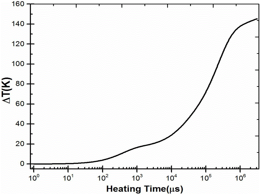
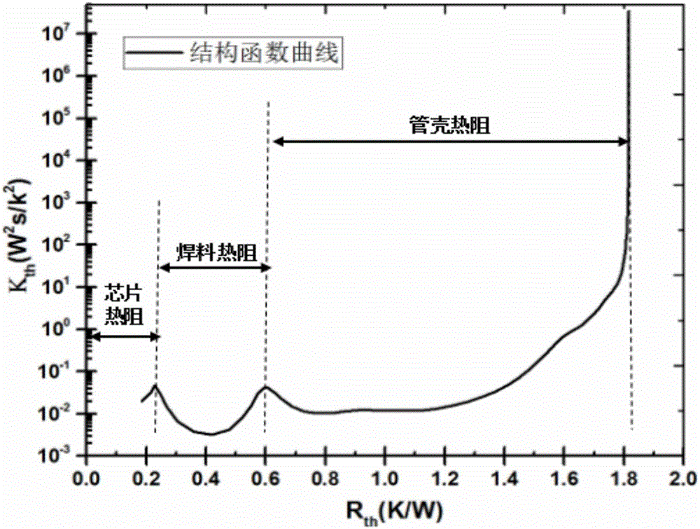
Image

Examples
Embodiment Construction
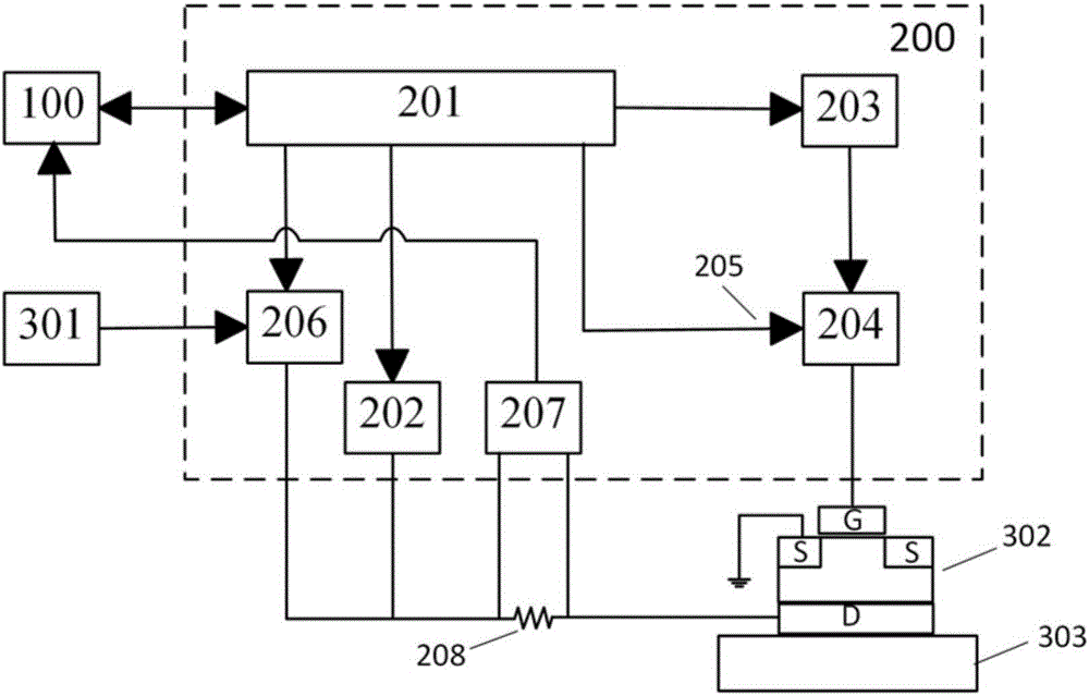
[0029] First, the power MOS device 302 to be tested is placed on a temperature-adjustable constant temperature platform 303 . After connecting the gate, source and drain wires of the power MOS device 302, the computer 100 is the control center, which realizes the transmission of signal instructions, transmission and storage of data. The computer 100 is connected to the FPGA unit 201 via USB, and the FPGA unit 201 is controlled by timing signals, respectively connected to the test current source 202, the grid-source operating voltage source 203, the grid-source operating power switch 204, the drain-source operating power switch 206, and the computer 100 is connected to the voltage and current acquisition unit 207 via USB.
[0030] During measurement, the control computer 100 issues an instruction, and the test current source 202 produces a test current identical to the temperature coefficient of the measured power MOS device, which is connected to the drain-source two ends of t...
PUM
 Abstract
Description
Claims
Application Information