Integrated circuit testing method

A technology of integrated circuits and testing methods, applied in the field of semiconductors, can solve problems such as the overall performance degradation of integrated circuits, and achieve the effect of preventing electrical breakdown

Active Publication Date: 2017-02-22
广西南宁市沃威机电设备有限公司
View PDF6 Cites 0 Cited by
  • Summary
  • Abstract
  • Description
  • Claims
  • Application Information

AI Technical Summary

Problems solved by technology

However, as the distance between adjacent devices becomes smaller and smaller, the influence between adjacent devices becomes more and more significant, and the influence of electrical parameters such as electromagnetic interference or inductance and capacitance mechanism between each other becomes greater and greater, resulting in integration Degradation of the overall performance of the circuit

Method used


Image

  • Integrated circuit testing method
  • Integrated circuit testing method
  • Integrated circuit testing method

Examples


Embodiment Construction

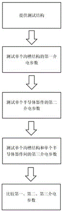
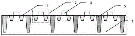
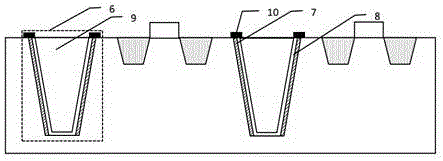
[0019] see figure 2 , the present invention provides an integrated circuit testing structure, comprising: a substrate 1; a plurality of discrete semiconductor devices 2 formed on the upper surface of the substrate 1; , a plurality of trench structures 6 located in the substrate 1, each of the plurality of trenches has a U-shaped cross-section, has a rectangular opening in plan view, and is adjacent to two opposite sides of the plurality of semiconductor devices And the bottom surface at the bottom of the groove; the two opposite electrode plate layers 7 arranged on the side; the trench isolation material 9 filled in the plurality of grooves and located on the electrode plate layer. It also includes a silicon carbide layer 8 between the electrode plate layer and the trench isolation material.

[0020] Wherein, the substrate 1 is a wafer or a silicon substrate, and has a certain thickness, which can form multiple devices and their auxiliary parts in post-production; the electr...


PUM


Abstract

The invention provides an integrated circuit testing method including (1) providing an integrated circuit testing structure; (2) testing a single trench isolation structure for a first dielectric parameter; (3) testing a single semiconductor device for a second dielectric parameter; (4) testing adjacent single trench isolation structures and the single semiconductor device for a third dielectric parameter; and (5) comparing the first, second and third dielectric parameters and evaluating the single trench isolation structure.

Description

technical field [0001] The invention relates to the technical field of semiconductors, in particular to a semiconductor testing method. Background technique [0002] With the improvement of the integration level of integrated circuits, the distance between devices in the circuit is getting smaller and smaller, and the influence between adjacent devices is getting bigger and bigger. [0003] Integrated circuits in the prior art often perform electrical isolation of multiple semiconductor devices through isolation trenches, for example, figure 1 The plurality of semiconductor devices 2 formed on the substrate 1 may be, for example, MOS devices, which include gate structures 3 and source / drains 4 , and the plurality of semiconductor devices 2 are dielectrically isolated by trenches 5 . However, as the distance between adjacent devices becomes smaller and smaller, the influence between adjacent devices becomes more and more significant, and the influence of electrical parameter...

Claims


Application Information

Patent Timeline
Patent Type & Authority Applications(China)
IPC IPC(8): G01R31/28H01L21/66
CPCG01R31/2851G01R31/2853H01L22/34
Inventor 张为凤
Owner 广西南宁市沃威机电设备有限公司
Why Eureka
Try Eureka