Passivation contact structure of selective polycrystalline silicon thin film and preparation method thereof
A polysilicon thin film, contact structure technology, applied in the direction of climate sustainability, final product manufacturing, sustainable manufacturing/processing, etc., can solve the problem of mass production of passivation contact technology, etc., to prevent damage to passivation contact, prevent The effect of current loss and efficiency improvement
- Summary
- Abstract
- Description
- Claims
- Application Information
AI Technical Summary
Problems solved by technology
Method used
Image

Examples
Embodiment 1
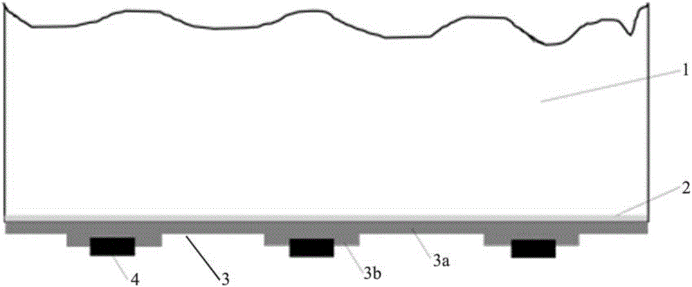
[0025] Such as figure 1 As shown, the passivation contact structure of the selective polysilicon thin film provided by the present invention is prepared with a layer of silicon dioxide layer 2 on the surface of crystalline silicon 1, the thickness of the silicon dioxide layer 2<2 nm, and on the surface of the silicon dioxide layer 2 A doped polysilicon film 3 is prepared on the surface, and the doped polysilicon film 3 has different thicknesses in different regions, specifically, the region without metal contact has a first thickness 3a, and the region with metal contact has a second thickness 3b, and the first The thickness 3a is smaller than the second thickness 3b, the range of the first thickness is 5-2000 nm, and the range of the second thickness is 30-70000 nm; the metal electrode 4 is formed on the surface of the second thickness region of the polysilicon film.
Embodiment 2
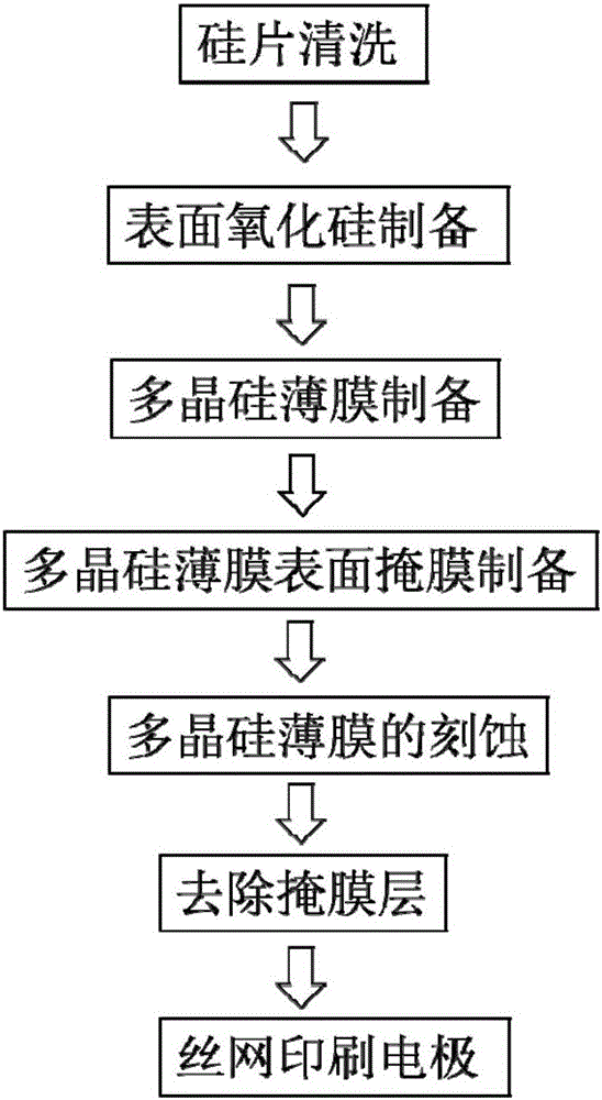
[0027] Such as figure 2 As shown, the preparation method of the passivation contact structure of the selective polysilicon thin film of the present embodiment comprises the following steps:
[0028] S1: Wafer cleaning:
[0029] S2: Preparation of surface silicon oxide: prepare a silicon dioxide layer with a thickness of 1.5 nm by thermal oxidation process;
[0030] S3: Preparation of polysilicon film: Deposit phosphorus-doped or boron-doped polysilicon film by low-pressure chemical vapor deposition (LPCVD), and the thickness of the polysilicon film is 200 nm;
[0031] S4: printing a mask on the surface of the polysilicon film;
[0032] S5: Etching of the polysilicon film: using HF / HNO3 solution to etch the polysilicon film to reduce its thickness to 70 nm to form a first thickness region;
[0033] S6: removing the mask layer, the unetched polysilicon thin film area under the mask layer is the second thickness area;
[0034] S7: Prepare electrodes: prepare metal electrodes...
Embodiment 3
[0036] Such as figure 2 As shown, the preparation method of the passivation contact structure of the selective polysilicon thin film of the present embodiment comprises the following steps:
[0037] S1: Wafer cleaning:
[0038] S2: Preparation of surface silicon oxide: prepare a silicon dioxide layer with a thickness of 1.3nm by hot nitric acid process;
[0039] S3: Preparation of polysilicon film: Deposit phosphorus-doped or boron-doped polysilicon film by low-pressure chemical vapor deposition (LPCVD), and the thickness of the polysilicon film is 100 nm;
[0040] S4: printing a mask on the surface of the polysilicon film;
[0041] S5: Etching of the polysilicon film: using HF / HNO3 solution to etch the polysilicon film to reduce its thickness to 50 nm to form a first thickness region;
[0042] S6: removing the mask layer, the unetched polysilicon thin film area under the mask layer is the second thickness area;
[0043] S7: Prepare electrodes: prepare metal electrodes on...
PUM
| Property | Measurement | Unit |
|---|---|---|
| Thickness | aaaaa | aaaaa |
| Thickness | aaaaa | aaaaa |
| Thickness | aaaaa | aaaaa |
Abstract
Description
Claims
Application Information
 - R&D Engineer
- R&D Manager
- IP Professional
- Industry Leading Data Capabilities
- Powerful AI technology
- Patent DNA Extraction
Browse by: Latest US Patents, China's latest patents, Technical Efficacy Thesaurus, Application Domain, Technology Topic.
© 2024 PatSnap. All rights reserved.Legal|Privacy policy|Modern Slavery Act Transparency Statement|Sitemap