High-power semiconductor laser chip conductive heat dissipation package heat sink

A semiconductor and laser technology, applied in the field of high-power semiconductor laser chip conduction heat dissipation package heat sink structure, can solve the problems of shortened device life, long heat dissipation path, decreased output efficiency, etc., to reduce thermal resistance and internal temperature rise, increase The effect of heat dissipation

Inactive Publication Date: 2017-02-22
CHANGCHUN UNIV OF SCI & TECH
View PDF4 Cites 2 Cited by
  • Summary
  • Abstract
  • Description
  • Claims
  • Application Information

AI Technical Summary

Problems solved by technology

The thermal saturation phenomenon is because the high-density heat generated when the laser is working is limited in the way of heat dissipation, and a large amount of heat accumulates in the chip, causing the temperature of the chip to rise significantly, resulting in an increase in the threshold current of the laser chip, a decrease in output efficiency, and a saturation or even drop in output power.
A higher chip temperature will also shorten the life of the device and become an important factor limiting the stability of semiconductor laser performance
[0003] The existing conduction heat dissipation packaging structure usually adopts C-mount heat sink, and its heat dissipation method is mainly through the heat dissipation surface at the bottom of the heat sink. The thermal resistance, which in turn affects the performance of the laser

Method used


Image

  • High-power semiconductor laser chip conductive heat dissipation package heat sink

Examples


Embodiment Construction

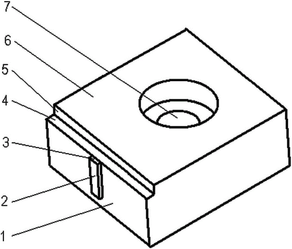
[0007] As shown in the accompanying drawings, the semiconductor laser chip conduction heat dissipation packaging heat sink has a chip welding surface (1), a stepped plane (4), a stepped elevation (5), and a fixing hole (7). The semiconductor laser chip (2) is welded on the chip welding surface (1), the light emitting end surface (3) of the chip is aligned with the step plane (4), and the fixing holes (7) are used to fix the heat sink to other heat dissipation surfaces. The steps composed of the step plane (4) and the step elevation (5) effectively increase the heat dissipation capacity of the semiconductor laser chip (2), and the smaller step plane (4) width and the larger step elevation (5) height have It is beneficial to obtain a smaller thermal resistance of the chip package.

[0008] The present invention is described below in conjunction with an example. The semiconductor laser chip (2) with a cavity length of 4mm and an output power of 10W is soldered to the chip welding...


PUM


Abstract

The invention relates to a high-power semiconductor laser chip conductive heat dissipation package heat sink and belongs to the technical field of laser. The main technical feature of the invention is that the heat dissipation efficiency of a laser chip is improved by the step structure of the heat sink. The invention keeps the advantages of simple structure, good working stability and convenient use of an existing conductive heat dissipation heat sink by means of structure optimization. Compared with the prior art, the high-power semiconductor laser chip conductive heat dissipation package heat sink obviously improves a heat dissipation path and improves the heat dissipation effect, and is suitable for the conductive heat dissipation package of most semiconductor laser chips.

Description

technical field [0001] The invention relates to a high-power semiconductor laser chip conduction heat dissipation package heat sink structure, which belongs to the technical field of semiconductor lasers. Background technique [0002] High-power semiconductor lasers have the advantages of small size, light weight, high electro-optic conversion efficiency, high reliability and long life. They have become the most promising laser light sources in the laser industry and are widely used in communications, industrial processing, medical treatment and materials. processing and other fields. The laser output power of high-power semiconductor laser chips is mainly limited by catastrophic optical cavity surface damage and thermal saturation. The thermal saturation phenomenon is because the high-density heat generated when the laser is working is limited in the way of heat dissipation, and a large amount of heat accumulates in the chip, causing the temperature of the chip to rise sig...

Claims


Application Information

Patent Timeline
Patent Type & Authority Applications(China)
IPC IPC(8): H01S5/024
CPCH01S5/02469
Inventor 张晓磊高欣乔忠良张晶薄报学
Owner CHANGCHUN UNIV OF SCI & TECH
Why Eureka
Try Eureka