Supercharge Your Innovation With Domain-Expert AI Agents!

A method of erasing NAND Flash

An erasing block and soft erasing technology, applied in information storage, static memory, instruments, etc., can solve the problems of inability to move the P-type semiconductor substrate 23 and fix it, so as to reduce charge traps and prolong service life , to ease the effect of offset

Active Publication Date: 2019-10-18
GIGADEVICE SEMICON (BEIJING) INC
View PDF5 Cites 0 Cited by
  • Summary
  • Abstract
  • Description
  • Claims
  • Application Information

AI Technical Summary

Problems solved by technology

The change of the threshold voltage of the floating gate 203 of the memory cell can affect the state change of the memory cell. It should be noted that the erasing and programming operations are opposite. In the existing erasing or programming operation method, one erasing or programming process applies Erase pulses or program pulses are constant
Based on the existing programming and erasing methods, some electrons do not have enough energy to reach the floating gate 203 during the process of tunneling to the floating gate during the programming operation, but are trapped in the tunnel oxide layer 24. During the erasing operation The electrons trapped in the tunnel oxide layer 24 cannot migrate from the tunnel oxide layer 24 to the P-type semiconductor substrate 23 after being erased by high voltage.

Method used


Image

  • A method of erasing NAND Flash
  • A method of erasing NAND Flash
  • A method of erasing NAND Flash

Examples


Embodiment 1

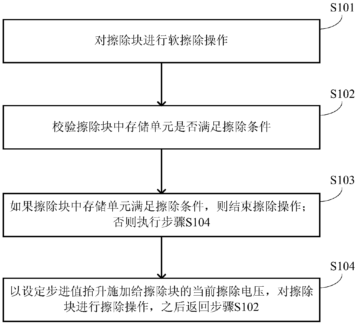
[0032] image 3 The flow chart of a kind of erasing method of Nand Flash that the embodiment 1 of the present invention provides, this method is carried out by Nand Flash, is a kind of improvement to existing erasing method, as image 3 As shown, the method includes:

[0033] Step S101 , performing a soft erase operation on the erase block.

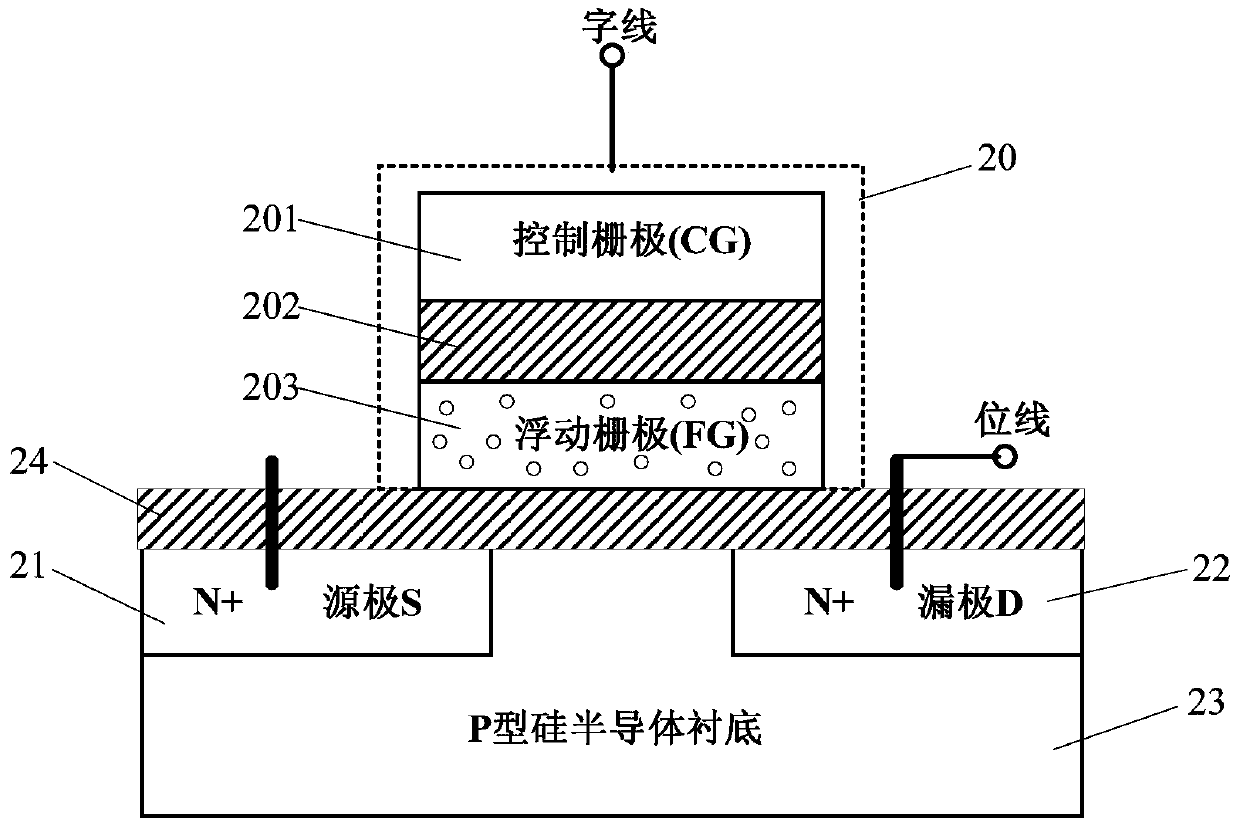
[0034] In this embodiment, the erasing block may specifically be a memory cell block used for erasing operations in the memory cell array of Nand Flash. The erasing operation is carried out in units of storage unit blocks, the storage unit array of the Nand Flash is composed of a plurality of storage unit blocks, the storage unit block is composed of a plurality of storage unit pages, and the storage unit pages are composed of a plurality of storage unit pages. Storage cells are connected in rows and columns. In a memory cell page, each row is connected by a plurality of memory cells with a word line, and each column is connected with ...

Embodiment 2

[0051] Figure 4 The flow chart of the erasing method of a kind of Nand Flash that the embodiment of the present invention provides, present embodiment optimizes on the basis of above-mentioned embodiment, in the present embodiment, the step is to erase block and carry out soft erase operation optimization as : a. Apply an initial soft erase voltage to the erase block, and continue to apply pressure within a preset time; b. Raise the current soft erase voltage with a set voltage increment value, and continue to apply it within the preset time. c. If the current soft erase voltage value does not reach the preset voltage value, repeat step b.

[0052] Further, before the step of applying the initial soft erase voltage for the erase block, a step is added:

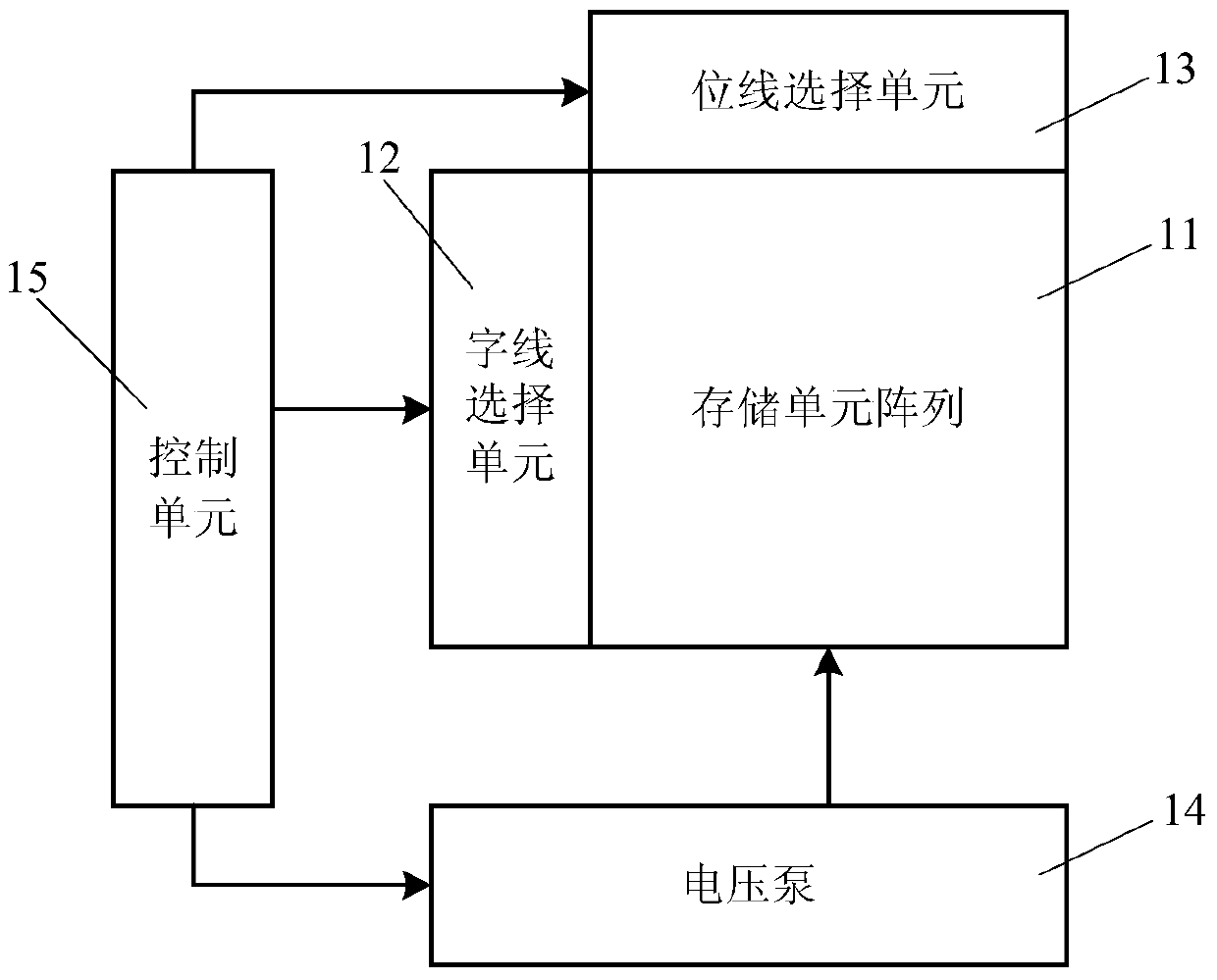
[0053] Based on the control unit in Nand Flash, the memory block to be erased is selected through word line selection and bit line selection, which is recorded as an erase block.

[0054] Correspondingly, the method of this...


PUM


Abstract

The invention discloses a Nand Flash erasing method. The method comprises the following steps: step 101, carrying out soft erasing operation on an erase block; step 102, examining whether memory units in the erase block satisfy the erasing conditions or not; step 103, if the memory units in the erase block satisfy the erasing conditions, stopping the erasing operation, and if the memory units in the erase block do not satisfy the erasing conditions, executing step 104; and step 104, lifting the current erasing voltage applied on the erase block according to a preset step value, carrying out erasing operation on the erase block, and returning to the step 102. The provided erasing method can reduce the charge traps in Nand Flash memory units during the erasing process, reduces the threshold voltage shift of memory units, and thus relieves the erasing degradation of Nand Flash, so the number of erasing is increased, and the service life is prolonged.

Description

technical field [0001] The invention relates to the technical field of storage device hardware, in particular to a method for erasing a Nand Flash. Background technique [0002] Nand Flash is a kind of Flash memory, which is a non-volatile memory device (Non-volatile Memory Device). It uses a non-linear macro-cell mode inside, which has the advantages of large capacity and fast rewriting speed, and is suitable for the storage of large amounts of data. figure 1 It is a simple structural diagram of Nand Flash in the prior art, which is composed of a memory cell array 11, a word line selection unit 12, a bit line selection unit 13, a voltage pump 14, and a control unit 15 of the entire Nand Flash chip, wherein the memory cell The array 11 includes memory cells arranged based on word lines and bit lines of each memory cell. Specifically, the memory cells are firstly connected by word lines and bit lines to form a page, then a plurality of pages are formed into a block, and fina...

Claims


Application Information

Patent Timeline
Patent Type & Authority Patents(China)
IPC IPC(8): G11C16/14G11C16/16
Inventor 潘荣华涂美红
Owner GIGADEVICE SEMICON (BEIJING) INC
Features
  • R&D
  • Intellectual Property
  • Life Sciences
  • Materials
  • Tech Scout
  • Unparalleled Data Quality
  • Higher Quality Content
  • 60% Fewer Hallucinations
Learn More