Substrate and manufacturing method thereof
A manufacturing method and substrate technology, applied in the fields of nonlinear optics, instruments, optics, etc., can solve the problems of reducing display effect, uneven surface of color resist layer, increasing production cost, etc., to avoid angular difference, smooth surface, and reduce height Effect
- Summary
- Abstract
- Description
- Claims
- Application Information
AI Technical Summary
Problems solved by technology
Method used
Image
Examples
Embodiment Construction
[0037] The following descriptions of the various embodiments refer to the accompanying drawings to illustrate specific embodiments in which the present invention can be practiced. The directional terms mentioned in the present invention, such as "up", "down", "front", "back", "left", "right", "inside", "outside", "side", etc., are for reference only The orientation of the attached schema. Therefore, the directional terms used are used to illustrate and understand the present invention, but not to limit the present invention. In the figures, structurally similar units are denoted by the same reference numerals.
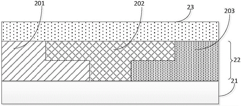
[0038] Please refer to figure 2 , figure 2 It is a schematic structural diagram of a substrate according to Embodiment 1 of the present invention.
[0039] The substrate in this embodiment may be a color filter substrate. Such as figure 2 As shown, the substrate includes a base substrate 21 , a color resist layer 22 and a transparent conductive layer 23 , wher...
PUM
 Abstract
Description
Claims
Application Information


