Manufacturing method of capacitive touch panel

A manufacturing method and touch panel technology, which are applied in the direction of electrical digital data processing, input/output process of data processing, instruments, etc., can solve the problems of long production cycle, low production efficiency and high production cost, so as to improve production efficiency and improve production efficiency. Reliable, flexible effects

Active Publication Date: 2017-03-15
BOE TECH GRP CO LTD +1
View PDF6 Cites 0 Cited by
  • Summary
  • Abstract
  • Description
  • Claims
  • Application Information

AI Technical Summary

Problems solved by technology

[0005] The film layer included in the capacitive touch panel is to deposit a film layer on the substrate first, and then perform a patterning process on the film layer to obtain the required shape and size. This production method has long production cycle, low production efficiency and low production cost. high

Method used


Image

  • Manufacturing method of capacitive touch panel
  • Manufacturing method of capacitive touch panel
  • Manufacturing method of capacitive touch panel

Examples


Embodiment 1

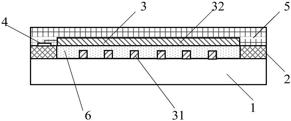
[0044] see figure 1 , an embodiment of the present invention provides a capacitive touch panel structure, including:

[0045] Substrate 1;

[0046] A light-shielding layer 2 is formed on the first surface of the substrate 1, and the first surface is any surface of the substrate 1;

[0047] A conductive layer 3 is formed on the first surface, and a metal layer 4 is formed on the first surface, the metal layer 4 is located on the side of the conductive layer 3, and the metal layer 4 is connected to the conductive layer 3;

[0048] A protective layer 5 is formed on the first surface, and the protective layer 5 covers the entire first surface, that is, covers the light shielding layer 2 , the protective layer 3 and the metal layer 4 .

[0049] Optionally, the conductive layer 3 includes a first conductive layer 31 and a second conductive layer 32; the first conductive layer 31 may be a horizontal conductive layer, and the second conductive layer 32 may be a vertical conductive l...

Embodiment 2

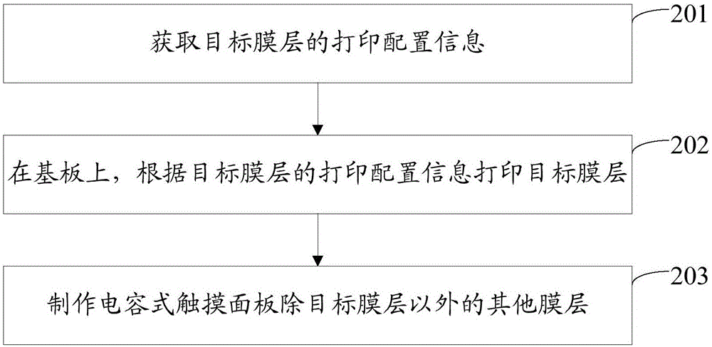
[0054] see figure 2 , a manufacturing method of a capacitive touch panel of the present invention, the manufacturing method comprising:

[0055] Step 201: Obtain the printing configuration information of the target film layer. The target film layer is a film layer in the capacitive touch panel whose area is smaller than the touch area of ​​the capacitive touch panel. The printing configuration information includes at least the position and shape of the target film layer on the substrate and / or size.

[0056] Step 202: On the substrate, print the target film layer according to the printing configuration information of the target film layer.

[0057] Step 203: Fabricate other film layers of the capacitive touch panel except the target film layer.

[0058] In the embodiment of the present invention, by obtaining the printing configuration information of the target film layer, according to the printing configuration information of the target film layer, the target film layer of...

Embodiment 3

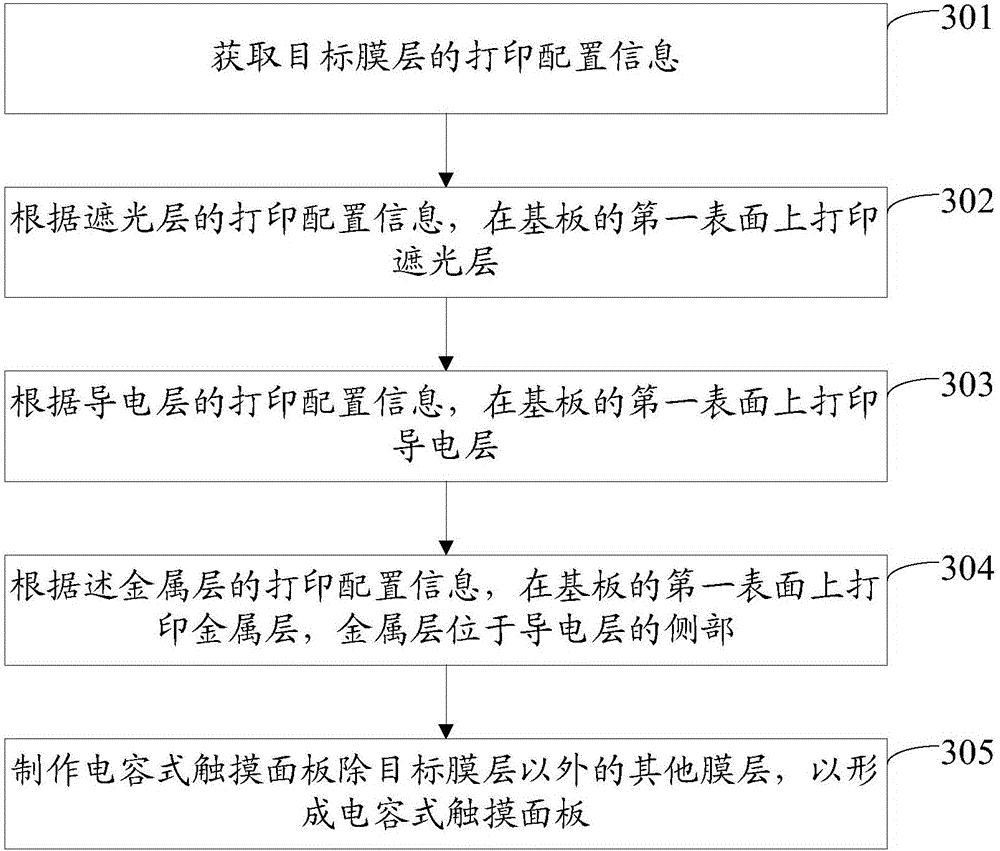
[0060] see image 3 , an embodiment of the present invention provides a method for manufacturing a capacitive touch panel, including:

[0061] Step 301: Obtain printing configuration information of a target film layer, where the target film layer is a film layer in a capacitive touch panel whose area is smaller than a touch area of ​​the capacitive touch panel.

[0062] The target film layer may include at least one of a light shielding layer, a conductive layer and a metal layer. In this step, the printing configuration information of the target film layer configured by the user may be received, and the printing configuration information includes information such as the position, shape and / or size of the target film layer on the substrate.

[0063]Users can define a coordinate system on the substrate in advance, and then configure the printing configuration information of the target film layer through this coordinate system. For example, see Figure 4 , define a coordinate...


PUM


Abstract

The invention discloses a manufacturing method of capacitive touch panel which belongs to the display field. The manufacturing method of capacitive touch panel comprises: the printing configuration information of the target membranous layer is obtained, wherein the target membranous layer is a membranous layer having a touch area smaller than the capacitive touch panel in the capacitive touch panel, and the printing configuration information includes at least the position, shape and / or size of the target membranous layer on the basilar plate; the target membranous layer is printed on the basilar plate according to the printing configuration information of the target membranous layer; and the other membranous layers of the capacitive touch panel are made except the target membranous layer. The method of capacitive touch panel has the advantages of shortening the production cycle, improving the production efficiency and reducing the production cost.

Description

technical field [0001] The invention relates to the display field, in particular to a method for manufacturing a capacitive touch panel. Background technique [0002] A capacitive touch panel is an input device capable of receiving finger touch signals. At present, many electronic devices are equipped with capacitive touch panels, and users can use the capacitive touch panels to control electronic devices. For example, currently there are capacitive touch panels on the display screens of many mobile phones, and users can operate the mobile phones by touching the capacitive touch screens. [0003] The capacitive touch panel includes multiple film layers. When making a capacitive touch panel, a certain film layer is deposited on the glass substrate first, and a patterning process is performed on the film layer to obtain the required shape and size; Deposit another film layer on the first layer, and perform a patterning process on the other film layer to obtain the required sh...

Claims


Application Information

Patent Timeline
Patent Type & Authority Applications(China)
IPC IPC(8): G06F3/044
CPCG06F3/044G06F2203/04103
Inventor 刘欢史文杰谢涛峰
Owner BOE TECH GRP CO LTD
Why Eureka
Try Eureka