

Board-level packaging structure and manufacturing method of a chip
A technology of packaging structure and manufacturing method, applied in semiconductor/solid-state device manufacturing, semiconductor/solid-state device parts, semiconductor devices, etc., can solve the problem of affecting the electrical performance of the IGBT chip packaging structure, unstable electrical performance of the device, uneven pressure, etc. question
- Summary
- Abstract
- Description
- Claims
- Application Information
AI Technical Summary
Problems solved by technology
Method used
Image

Examples
Embodiment 1
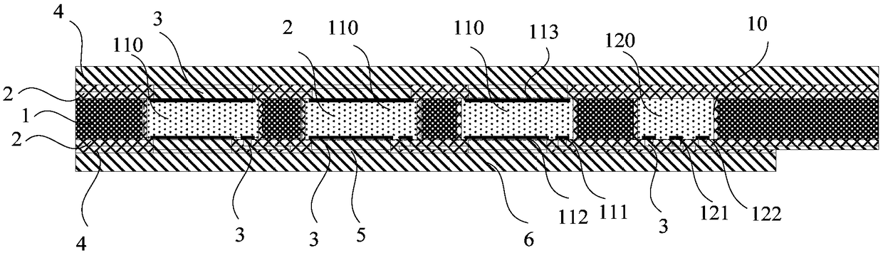
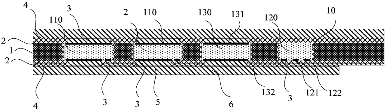
[0042] figure 1 It is a schematic diagram of a board-level package structure of a chip provided by Embodiment 1 of the present invention. figure 2 It is a schematic diagram of a board-level package structure of a chip provided by Embodiment 1 of the present invention.
[0043] Embodiments of the present invention provide a chip board-level packaging structure, such as figure 1 As shown, the structure includes: a substrate 1 on which at least two accommodating spaces 10 are formed, and the accommodating spaces 10 penetrate the substrate 1 . At least one IGBT chip 110 and at least one driver chip 120 embedded in the accommodation space 10 , the IGBT chip 110 and the driver chip 120 are respectively embedded in the corresponding accommodation space 10 . The first dielectric layer 2 formed on the surface of the substrate 1, the IGBT chip 110 and the driver chip 120, at least part of the electrodes of the IGBT chip 110 and the driver chip 120 are exposed and covered with the fir...
Embodiment 2
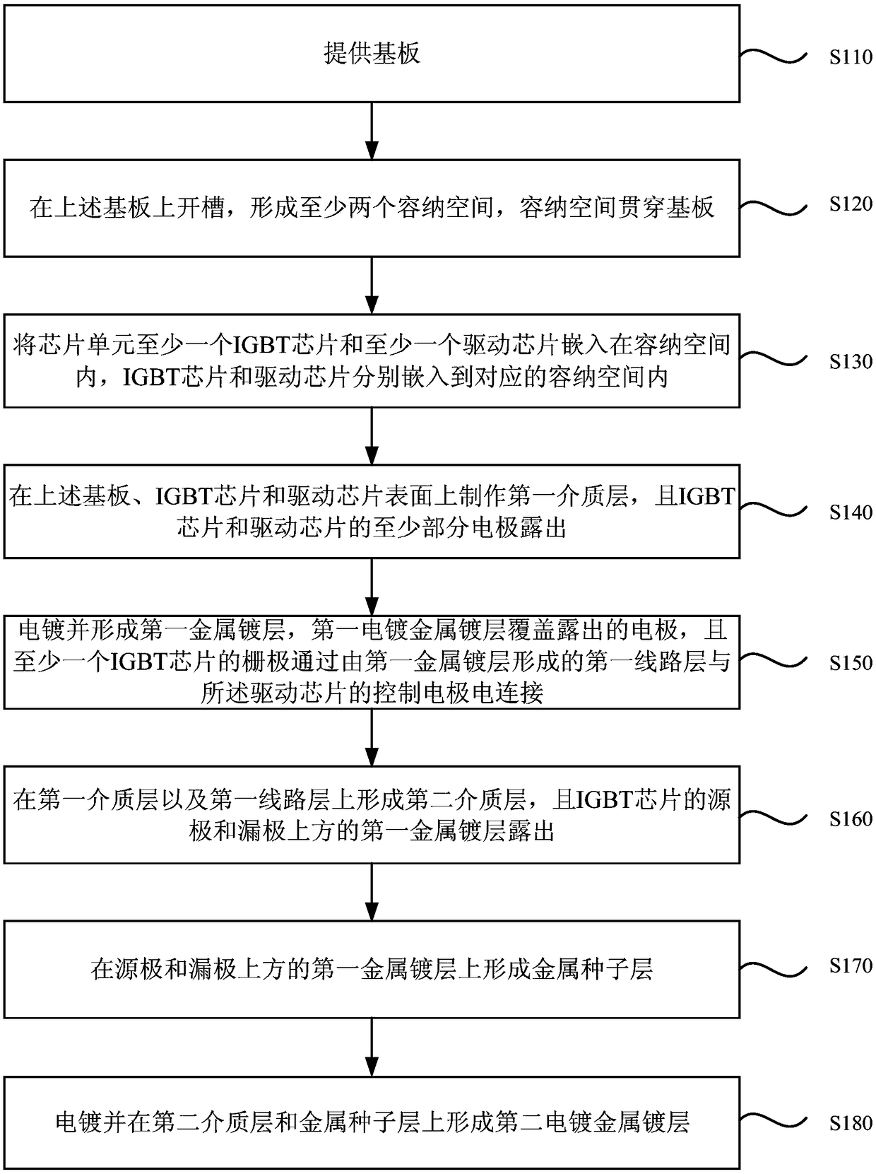
[0052] image 3 It is a schematic flowchart of a manufacturing method of a board-level packaging structure of a chip provided by Embodiment 2 of the present invention; Figure 4a-Figure 4j It is a cross-sectional view corresponding to each step of a manufacturing method of a chip board-level packaging structure provided in Embodiment 2 of the present invention.
[0053] On the basis of the above examples, refer to image 3 , an embodiment of the present invention provides a method for manufacturing a board-level packaging structure of a chip, the method comprising the following steps:
[0054] Step S110 , providing a substrate.
[0055] refer to Figure 4a , providing a substrate 1 . Exemplarily, the substrate 1 may be a metal molybdenum plate or an organic resin material.
[0056] Step S120, making grooves on the above-mentioned substrate to form at least two accommodating spaces, and the accommodating spaces penetrate the substrate;
[0057] refer to Figure 4b , groo...
PUM
 Abstract
Description
Claims
Application Information