Chip mounting machine and mounting method

A placement machine and chip technology, applied in the direction of electrical components, electrical components, etc., can solve the problem of poor temperature stability of the panel, achieve smooth adsorption and uniform heating, improve the accuracy and efficiency of chip placement, and improve the stability of the effect

Inactive Publication Date: 2017-03-22
CETC BEIJING ELECTRONICS EQUIP
View PDF2 Cites 6 Cited by
  • Summary
  • Abstract
  • Description
  • Claims
  • Application Information

AI Technical Summary

Problems solved by technology

[0004] The purpose of the embodiments of the present invention is to provide a chip mounter and a mount method, which solves the problem of poor temperature stability of the panel during the chip mount process

Method used


Image

  • Chip mounting machine and mounting method
  • Chip mounting machine and mounting method
  • Chip mounting machine and mounting method

Examples


Embodiment Construction

[0025] In order to make the technical problems, technical solutions and advantages to be solved by the present invention clearer, the following will describe in detail with reference to the drawings and specific embodiments.

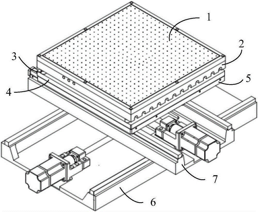
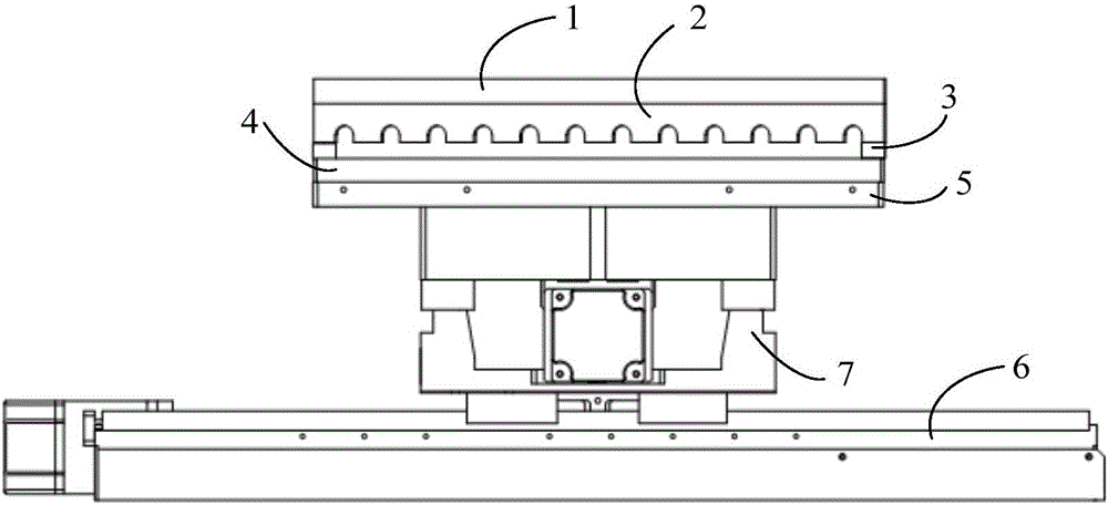
[0026] Such as Figure 1-6 As shown, the embodiment of the present invention provides a chip mounter, including:

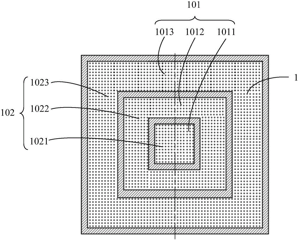
[0027] Adsorption device 1, the adsorption device 1 is provided with at least one layer of vacuum-tight wall 101 and at least one vacuum adsorption area 102, wherein, the material selected for each of the vacuum adsorption areas 102 is a porous material with high open porosity, and each hole inside Interconnected with each other to form a network structure, each vacuum adsorption area 102 corresponds to a layer of vacuum sealing wall 101, and the adsorption device 1 is used to place the panel;

[0028] The heating device 2, the heating device 2 is arranged below the adsorption device 1, and the upper surface of the heating device 2 is close...


PUM


Abstract

The invention provides a chip mounting machine and a mounting method. The chip mounting machine comprises an adsorption device, a heating device and a vacuum device. At least one layer of vacuum sealing wall and at least one vacuum adsorption region are arranged on the adsorption device. Each of the vacuum adsorption regions is made of special multihole materials. The adsorption device is used for loading a panel. The heating device is arranged under the adsorption device. The upper surface of the heating device is tightly attached to the lower surface of the adsorption device. Multiple uniformly arranged installation holes and heating bodies filling the installation holes are arranged in/on the lower surface of the heating device. Multiple vacuum hole channels are arranged on the heating device and correspond to and communicate with the vacuum adsorption region. The vacuum device is connected with and communicates with the vacuum hole channels. In this way, stable adsorption and uniform heating of big and thin chip panels can be achieved, so stability of mounting temperature and chip mounting precision and efficiency during the chip mounting process are improved.

Description

technical field [0001] The invention relates to the field of chip mounting, in particular to a chip mounting machine and a mounting method. Background technique [0002] With the rapid development of global electronic information technology, consumers need smaller portable electronic products, which makes the chip placement technology constantly updated. The chip bonding process mainly includes chip-to-chip, chip-to-substrate and chip-to-panel packaging technologies. During the chip-to-panel chip mounting process, in order to ensure the mounting quality and accuracy, the panel needs to rise to the temperature required for mounting. Then proceed to the placement process. [0003] At present, when performing the chip-to-panel chip mounting process, the preheating function of the panel before mounting is generally realized on the heating table. After the preheating is completed, the panel is moved to the workbench for bonding and placement. During the process of moving the pa...

Claims


Application Information

Patent Timeline
Patent Type & Authority Applications(China)
IPC IPC(8): H05K13/04
CPCH05K13/0408H05K13/046
Inventor 叶乐志郎平王军帅
Owner CETC BEIJING ELECTRONICS EQUIP
Why Eureka
Try Eureka