A kind of high-resistivity single crystal ZnO-based radiation detection device and its preparation method and application

A radiation detector and high resistivity technology, applied in the field of radiation detectors, can solve problems such as difficult to guarantee the stability and reliability of device performance, limit the application of detector devices, and weak radiation resistance, and achieve good promotion and application prospects. Uniform and controllable film thickness, strong radiation resistance

Active Publication Date: 2018-04-24
SUN YAT SEN UNIV
View PDF8 Cites 0 Cited by
  • Summary
  • Abstract
  • Description
  • Claims
  • Application Information

AI Technical Summary

Problems solved by technology

[0004] However, both silicon and germanium are sensitive to ambient temperature and have weak radiation resistance due to their narrow band gaps, so their use in systems working in space environments is greatly limited.
On the other hand, for compound semiconductors, such as III-V group compounds GaAs, InGaAs, GaN, II-VI group compounds CdTe (energy resolution 0.3%@662keV gamma rays, requires Peltire cooling), CdZnTe, VII-B group II Halogen compounds HgI2, PbI2, TlBr and their ternary compounds HgCdTe, etc. Most of these materials have the disadvantages of low melting point, easy decomposition, and weak radiation resistance. Based on the stability and reliability of the device performance It is difficult to ensure that these problems greatly limit the application of related detection devices in harsh environments such as nuclear power plants and space

Method used


Image

  • A kind of high-resistivity single crystal ZnO-based radiation detection device and its preparation method and application
  • A kind of high-resistivity single crystal ZnO-based radiation detection device and its preparation method and application
  • A kind of high-resistivity single crystal ZnO-based radiation detection device and its preparation method and application

Examples


Embodiment 1

[0059] 1. Preparation of high resistivity ZnO single crystal

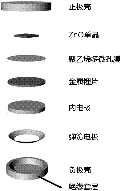
[0060] (1) Press a 10 cm square high-quality low-resistance zinc oxide wafer in an argon-filled glove box at room temperature figure 1 The shown sequence was assembled into a commercial CR 2032 battery case, where the electrolyte used was a 1M LiPF6 solution dispersed in a 4:3:3 mixed solution of ethylene carbonate, ethyl methyl carbonate and diethyl carbonate , using Celgard 2400 polyethylene microporous membrane as the electronic separator.

[0061] The implantation of lithium into the ZnO single crystal was realized by the constant current discharge treatment at room temperature by the LAND BT2013A multi-channel battery test system.

[0062] The thickness of the high-quality low-resistance zinc oxide wafer used in this example is 0.3 mm, the constant-current discharge current is set to 3 microamps, and the discharge time is set to 15 hours.

[0063] (2) The lithium-infused zinc oxide wafer processed in the abo...

Embodiment 2

[0075] 1. Preparation of high resistivity ZnO single crystal, the method is the same as that of Example 1.

[0076] 2. Preparation of high-resistivity single-crystal ZnO-based radiation detection devices

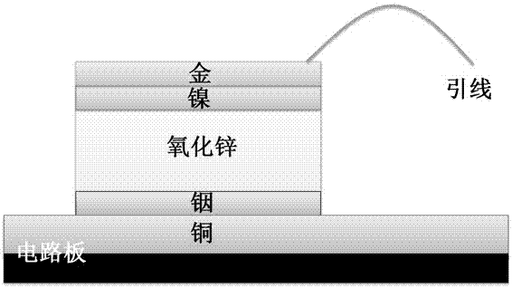
[0077] Using thermal / electron beam evaporation method, according to Figure 4 In the sequence shown, a double-layer metal electrode of 35 nm titanium and 20 nm gold vapor-deposited on one side surface of a high-resistivity ZnO wafer.

[0078] A thicker metal indium electrode is then plated on the other side of the ZnO wafer.

[0079] The electrodes on both sides form good electrical contact.

[0080] The wafer is bonded to the circuit board using molten indium by heating the device. And connect the chip to the circuit board through gold wires.

[0081] 3. Test

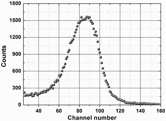
[0082] The obtained high-resistance ZnO-based detection device is placed in a vacuum, thereby reducing the energy loss of alpha particles during flight. Detector response testing using from 243 Am- 244 The Cm...


PUM


Abstract

Provided are a high-resistivity monocrystalline ZnO-based radiation detection device, a preparation method therefor, and an application thereof. The preparation method comprises the following steps: S1. preparing a high-resistivity monocrystalline ZnO chip; S2. vapor-depositing metal electrode layers on two sides of the high-resistivity monocrystalline ZnO chip; and S3. combining the chip treated in S2 onto a circuit board, and connecting the chip to the circuit board by means of a gold thread. Moreover, the device performance is tested using an α source, and the device shows an effective radiation response. According to the method, the radiation detection device is prepared using a high-resistivity ZnO material of excellent characteristics such as high irradiation resistance, wide band gap, and high breakdown electric field intensity. The obtained device is simple in structure, simple in manufacturing process, low in costs, and high in repeatability and quality, and has high practicality and a good promoting and application prospect.

Description

technical field [0001] The invention belongs to the technical field of radiation detectors. More specifically, it relates to a high-resistivity single-crystal ZnO-based radiation detection device and its preparation method and application. Background technique [0002] In many military, national defense, aerospace and other fields, detectors need to have high sensitivity, miniaturization, and strong radiation resistance. Compared with the average radiation energy (~30eV) required by conventional gas radiation detectors to generate detection signals through gas ionization, the average radiation energy required for semiconductor materials to generate a pair of electron-hole pairs is <10eV, so at the same radiation energy Especially for weak signals, the sensitivity of semiconductor materials is higher than that of gases; at the same time, because the density of semiconductor materials is higher than that of gases, a very thin layer of semiconductor materials (a few microns...

Claims


Application Information

Patent Timeline
Patent Type & Authority Patents(China)
IPC IPC(8): H01L31/18H01L31/0224H01L31/0296H01L31/08
CPCH01L31/0224H01L31/0296H01L31/085H01L31/1828C30B29/16H01L31/08H01L31/18Y02P70/50
Inventor 黄丰季旭董美严崐
Owner SUN YAT SEN UNIV
Why Eureka
Try Eureka