High-resistivity single crystal zinc oxide wafer based radiation detector and preparation method and use thereof

a radiation detector and high-resistivity technology, applied in the field of radiation detectors, can solve the problems of low melting point, easy decomposition, weak anti-irradiation capability, and difficult to guarantee the stability and reliability of the device constructed based on these materials, and achieves low cost, high resistance, and simple operation

Active Publication Date: 2019-04-18
SUN YAT SEN UNIV
View PDF0 Cites 0 Cited by
  • Summary
  • Abstract
  • Description
  • Claims
  • Application Information

AI Technical Summary

Benefits of technology

The present invention provides a novel and simple method to prepare high-resistivity single crystal ZnO for a radiation or photoelectric detector. This method uses an electrochemical method combined with an annealing treatment to obtain an ultra-high resistivity single crystal ZnO wafer. This ZnO material has excellent characteristics such as a superior anti-irradiation capability, a wider band gap, and higher breakdown electric field strength. The obtained device has a good radiation response and has a simple structure, a low cost, and high repeatability. The invention utilizes a high-resistant ZnO material to manufacture a radiation detector. The invention provides an improved method of thermal evaporation or electron beam evaporation for the deposition of high-quality film onto various electrodes. The invention also uses a single-energy alpha source with a low beam current as a radiation source for better sensitivity and energy discrimination of the detector.

Problems solved by technology

However, both silicon and germanium are sensitive to ambient temperature and weak in radiation resistance due to their narrow band gap, so it is greatly restricted to equip them into a system working in space environment.
On the other hand, for compound semiconductors, such as Group III-V compound GaAs, InGaAs and GaN, Group II-VI compound CdTe (energy resolution 0.3% @ 662 keV gamma ray, requires Peltire refrigeration) and CdZnTe, Group VII-B dibasic halogen compounds HgI2, PbI2, TlBr and their ternary compound HgCdTe, etc., most of these materials have the disadvantages of low melting point, easy decomposition, and weak anti-irradiation capability, and stability and reliability of performance of the device constructed based on these materials is difficult to guarantee.
These problems greatly limit the application of related detectors in harsh environments such as nuclear power plant and space.
However, how to obtain high resistivity and thereby strongly suppress dark current noise in order to obtain high-resistivity single crystal ZnO with high signal-to-noise ratio has been an important obstacle hindering its application in the field of radiation detection.

Method used


Image

  • High-resistivity single crystal zinc oxide wafer based radiation detector and preparation method and use thereof
  • High-resistivity single crystal zinc oxide wafer based radiation detector and preparation method and use thereof
  • High-resistivity single crystal zinc oxide wafer based radiation detector and preparation method and use thereof

Examples


embodiment 1

[0061]1. Preparation of High-Resistivity ZnO Single Crystal

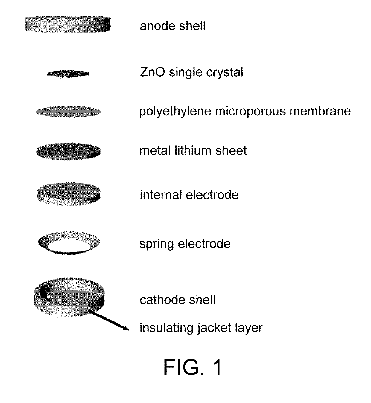
[0062](1) A high-quality low-resistance zinc oxide wafer of 10 centimeter squares was assembled into a commercial CR 2032 battery case in the order shown in FIG. 1 at room temperature in an argon-filled glove box, an electrolyte used was a 1 M LiPF6 solution dispersed in a mixed solution of ethylene carbonate, ethyl methyl carbonate and diethyl carbonate in a volume ratio of 4:3:3, and a Celgard 2400 polyethylene microporous membrane was used as an electronic diaphragm.

[0063]A LAND BT2013A multi-channel battery testing system performed a constant-current discharge treatment at room temperature to realize an injection of lithium into the ZnO single crystal.

[0064]A thickness of the high-quality low-resistance zinc oxide wafer used was 0.3 millimeters, a constant current discharge current was set to 3 μA, and a discharge time was set to 15 hours.

[0065](2) The lithium-injected zinc oxide wafer treated in the above step (1) was p...

embodiment 2

[0068]1. Preparation of high-resistivity single crystal ZnO

[0069]The method differed from Embodiment 1 in that the thickness of the ZnO wafer in the step (1) was 0.2 millimeters, the constant current discharge current was set to 3 μA, and the discharge time was set to 10 hours.

[0070]Compared with Embodiment 1, this Embodiment shortened the discharge time due to a reduction of the thickness of the wafer, thereby obtaining a same processing result.

[0071]2. The high-resistivity ZnO single crystal wafer prepared by this Embodiment had a resistivity of 1011 Ωcm, which was 1011 higher than that before treatment.

embodiment 3

[0072]1. Preparation of high-resistivity single crystal ZnO

[0073]The method differed from Embodiment 1 in that the thickness of the ZnO wafer in the step (1) was 0.5 millimeters, the constant current discharge current was set to 3 μA, and the discharge time was set to 25 hours.

[0074]Compared with Embodiment 1, this Embodiment prolonged the discharge time due to an increase in the thickness of the wafer, thereby obtaining the same processing result.

[0075]2. The high-resistivity ZnO single crystal wafer prepared by this Embodiment had a resistivity of 1011 Ωcm, which was 1011 higher than that before treatment.


PUM

PropertyMeasurementUnit
volume ratioaaaaaaaaaa
pressureaaaaaaaaaa

Abstract

The present invention discloses a high-resistivity single crystal zinc oxide (ZnO) wafer and a high-resistivity single crystal ZnO-based radiation detector, and preparation method and use thereof. The preparation method of the high-resistivity single crystal zinc oxide wafer is to place a single crystal ZnO wafer in a metal lithium electrochemical device for a constant-current discharge treatment, and then to place the single crystal ZnO wafer in a high-pressure oxygen atmosphere at 800 to 1000° C. and 10 to 30 atm for an annealing treatment for 20 to 28 hours. The preparation method of the radiation detector is to evaporate a metal electrode layer at both sides of the high-resistivity single crystal ZnO wafer, then to bond the wafer onto a circuit board, and to connect the wafer with the circuit board by a gold thread.

Description

CROSS-REFERENCE TO RELATED APPLICATION[0001]This application is a continuation of international PCT application serial no. PCT / CN2016 / 095816, filed on Aug. 18, 2016, which claims the priority benefit of China application no. 201610612939.2, filed on Jul. 29, 2016, and a continuation of international PCT application serial no. PCT / CN2016 / 095817, filed on Aug. 18, 2016, which claims the priority benefit of China application no. 201610612940.5, filed on Jul. 29, 2016. The entirety of each of the above-mentioned patent applications is hereby incorporated by reference herein and made a part of this specification.TECHNICAL FIELD[0002]The present invention belongs to the technical field of radiation detector, and more specifically, relates to a high-resistivity single crystal zinc oxide wafer and a radiation detector, and a preparation method and use thereof.BACKGROUND[0003]In many fields of military, national defense, aerospace, etc., detectors need to have characteristics such as high se...

Claims


Application Information

Patent Timeline
Patent Type & Authority Applications(United States)
IPC IPC(8): H01L31/18C30B29/16C30B33/04H01L31/0296H01L31/08H01L31/0224H01L31/02
CPCH01L31/1828C30B29/16C30B33/04H01L31/0296H01L31/085H01L31/0224H01L31/02002
Inventor HUANG, FENGJI, XUDONG, MEIYAN, KUN
Owner SUN YAT SEN UNIV
Why Eureka
Try Eureka