Thermal radiation infrared transmitting and probing integrated device

An infrared emission and integrated device technology, which is used in the measurement of fluid velocity using thermal variables, the application of thermal effects to detect fluid flow, instruments, etc., to achieve the effects of simple manufacturing process, reduction of thermal stress, and simple structure

Inactive Publication Date: 2011-01-19
HUAZHONG UNIV OF SCI & TECH
View PDF5 Cites 15 Cited by
  • Summary
  • Abstract
  • Description
  • Claims
  • Application Information

AI Technical Summary

Problems solved by technology

Since the emission characteristics are greatly affected by the size parameters of the microstructure pattern, this method also has the stability of the emi

Method used


Image

  • Thermal radiation infrared transmitting and probing integrated device
  • Thermal radiation infrared transmitting and probing integrated device
  • Thermal radiation infrared transmitting and probing integrated device

Examples


Example Embodiment

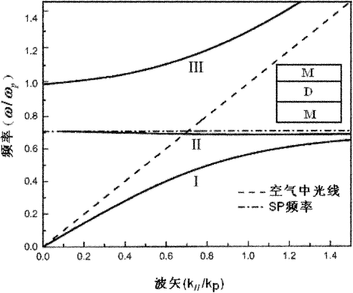
[0018] The basic optical multilayer structure of the narrow-band thermal infrared emission and infrared absorption integrated device of the present invention adopts the MDM structure, where M represents a conductive layer such as a metal or non-metal conductive compound, and D represents an insulating or semiconductor dielectric layer, which can be one or more Combination layers of dielectric materials. The basic principle is that when thermally excited radiation or external incident radiation coupling in the structure excites the SPP mode in the MDM, the SPP mode will be confined in the dielectric layer D to enhance emission or absorption. The SPP mode in the MDM structure can be divided into three types, corresponding to figure 1 The curves of Ⅰ, Ⅱ and Ⅲ in the MDM dispersion relation shown, figure 1 Ω in p And k p Are the plasma frequency and wave vector in M, ω SP Is the frequency of the excited SPP mode. It is noteworthy that figure 1 The patterns represented by the type...


PUM

PropertyMeasurementUnit
Resistivityaaaaaaaaaa
Thicknessaaaaaaaaaa
Thicknessaaaaaaaaaa

Abstract

The invention discloses a thermal radiation infrared transmitting and probing integrated device. The integrated device is in the structure that: a silicon substrate provided with a substrate insulation layer is opened with at least one thermal isolation cavity, the thermal isolation cavity is suspended with at least one transmitting unit and at least one probing unit which are adjacent and are arranged side by side, the transmitting unit is connected with the silicon substrate by virtue of at least two supporting arms, and the probing unit is connected with the silicon substrate by virtue of at least two supporting arms. The transmitting unit comprises a first insulation layer, a non metal conductive layer, a first medium layer and a first surface conductive layer which are superposed from the bottom to the top; and the probing unit comprises a second insulation layer, a metal conductive layer, an isolation layer, an infrared sensitive layer and a photonic crystal microstructure layer which are superposed from the bottom to the top. The integrated device has the advantages of simple structure, stable high temperature properties and adjustable wavelength, and narrow-band absorption probing narrower than the width of wavelength spectrum of the transmitting unit can be obtained. The integrated device of the invention can be applied to infrared gas sensor and infrared spectrometer.

Description

technical field [0001] The invention belongs to radiation generation and detection technology, and relates to an infrared emission device generated by thermal radiation and a detection device for infrared radiation, especially an integration of a high-temperature narrow-band thermal infrared emission unit and a thermal radiation detection unit manufactured by micro-electromechanical system (MEMS) technology device. Background technique [0002] Non-dispersive infrared (NDIR) gas sensors use the infrared characteristic absorption of gases for gas measurement. The principle is based on Lambert Beer's law, that is, if infrared light is irradiated on a gas with more than two molecules, the kinetic energy of the molecules will change and absorb light of a specific wavelength. This specific wavelength of light is determined by the molecular structure and judged by the absorption spectrum. Molecular species, gas concentration can be measured by the intensity of absorption. Compar...

Claims


Application Information

Patent Timeline
IPC IPC(8): G01N21/35B81B1/00G01N21/3504
Inventor 赖建军叶红
Owner HUAZHONG UNIV OF SCI & TECH
Why Eureka
Try Eureka