
Flexible circuit board and manufacturing method thereof

A technology of flexible circuit boards and conductive circuit layers, applied in the direction of flexible printed circuit boards, printed circuit manufacturing, printed circuits, etc., can solve the problems of large dielectric loss and large signal attenuation, and achieve the goal of reducing signal attenuation and ensuring stability Effect

Active Publication Date: 2017-04-19
QING DING PRECISION ELECTRONICS HUAIAN CO LTD +1
View PDF5 Cites 3 Cited by
  • Summary
  • Abstract
  • Description
  • Claims
  • Application Information

AI Technical Summary

Problems solved by technology

However, the dielectric loss of the above materials is still relatively large, resulting in a large signal attenuation in the transmission line of the circuit board made of the above materials

Method used


Image

  • Flexible circuit board and manufacturing method thereof
  • Flexible circuit board and manufacturing method thereof
  • Flexible circuit board and manufacturing method thereof

Examples


Embodiment Construction

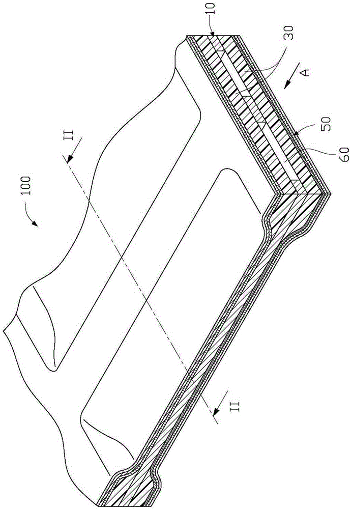
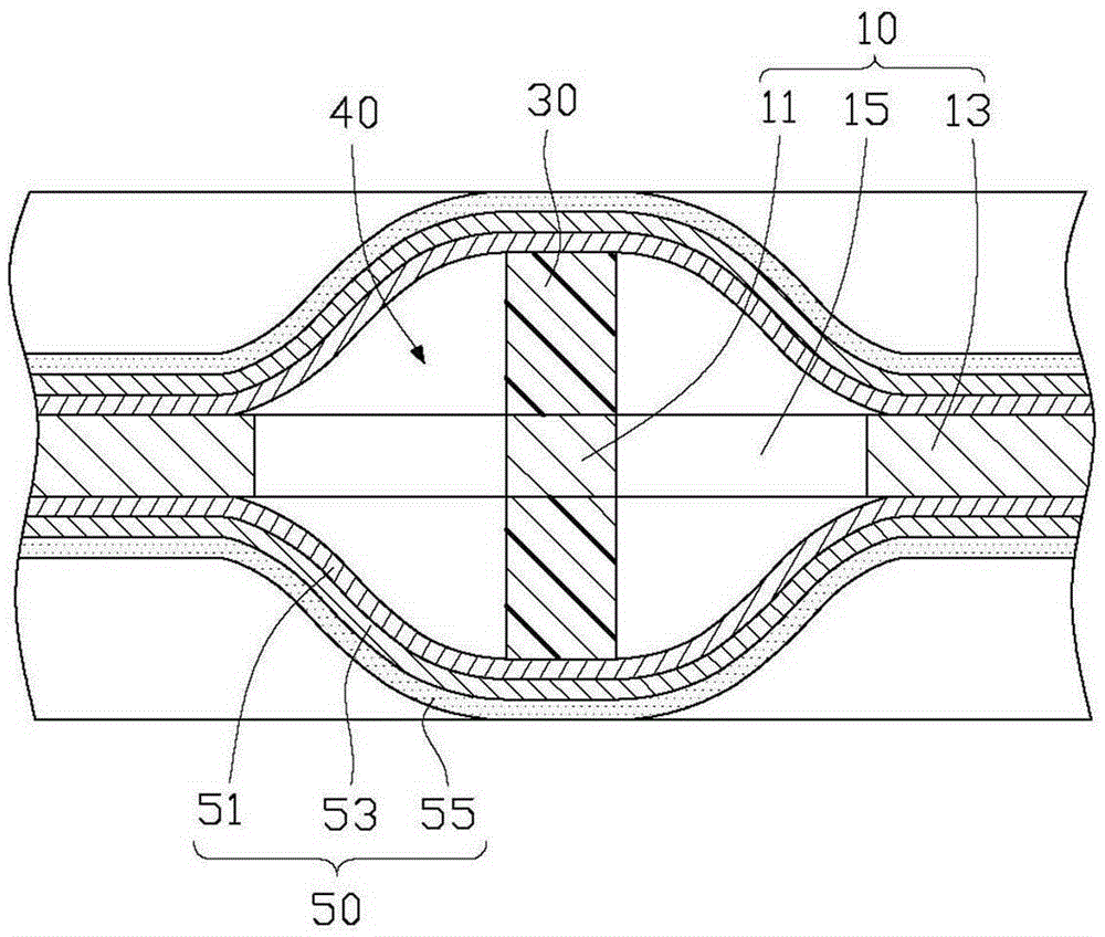
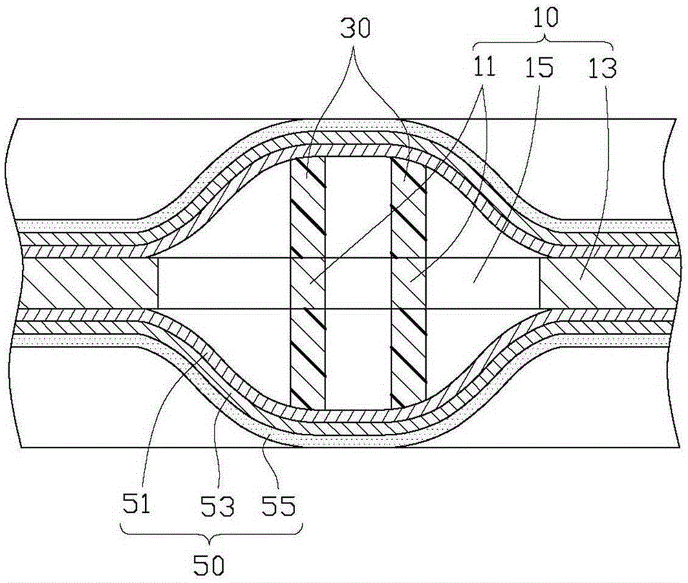
[0022] see figure 1 , the flexible circuit board 100 of the preferred embodiment of the present invention includes a conductive circuit layer 10, two photosensitive resin layers 30 respectively formed on the opposite surfaces of the conductive circuit layer 10 and covering the conductive circuit layer 10 and the photosensitive resin layer 30 of the two electromagnetic shielding layers 50.

[0023] see figure 2 The conductive circuit layer 10 includes at least one signal line 11 , two ground lines 13 respectively located on two sides of the signal line 11 , and at least two gaps 15 . The gap 15 is used to separate the signal lines 11 and / or between the signal lines 11 and the grounding line 13 . In this embodiment, the conductive circuit layer 10 only includes a signal line 11 , two ground lines 13 and two gaps 15 . The two gaps 15 are respectively located between the signal line 11 and one of the ground lines 13 for separating the signal line 11 from the ground line 13 . ...


PUM


Abstract

A flexible circuit board comprises a conductive line layer, two photosensitive resin layers and two electromagnetic shielding layers. The conductive line layer comprises at least one signal line, two grounding lines located on two sides of the signal line respectively and at least two gaps. Each gap comprises two opening portions located on two end portions of the corresponding signal line respectively. The two photosensitive resin layers cover two opposite surfaces of the signal line, cover the opening portions respectively and are combined with each end portion of the grounding lines. The two electromagnetic shielding layers cover surfaces of the two photosensitive resin layers, the grounding lines and the gaps, wherein the surfaces of the two photosensitive resin layers are far away from the signal lines; the grounding lines do not combine with the photosensitive resin layers; and the gaps are not covered by the photosensitive resin layers. Therefore, the electromagnetic shielding layers, the photosensitive resin layers, the signal lines and the grounding lines commonly surround areas of each gap so as to form an accommodation chamber, wherein the areas of each gap are not covered by the photosensitive resin layers. Each accommodation chamber is connected to the two opening portions of the corresponding gap so as to form a chamber.

Description

technical field [0001] The invention relates to a flexible circuit board and a manufacturing method thereof. Background technique [0002] The signal attenuation on the high-frequency transmission signal line mainly comes from the attenuation caused by the dielectric loss, wherein the dielectric loss is proportional to the dielectric loss factor and the dielectric constant. The manufacturing method of radio frequency circuit boards in the industry usually uses liquid crystal polymer (Liquid Crystal Polymer, LCP), Teflon (Teflon) or pure rubber as the base material for covering signal lines. However, the dielectric loss of the above-mentioned materials is still relatively large, resulting in relatively large signal attenuation in the transmission line of the circuit board made of the above-mentioned materials. Contents of the invention [0003] In view of this, it is necessary to provide a flexible circuit board with little signal attenuation. [0004] In addition, it is ...

Claims


Application Information

Patent Timeline
IPC IPC(8): H05K1/02H05K3/06
CPCH05K1/0218H05K3/06H05K2201/0723H05K1/0221H05K1/024H05K3/4697H05K2201/05H05K2201/0715H05K1/0219H05K1/0296H05K3/022
Inventor 胡先钦何明展
Owner QING DING PRECISION ELECTRONICS HUAIAN CO LTD
Features
  • Generate Ideas
  • Intellectual Property
  • Life Sciences
  • Materials
  • Tech Scout
  • Unparalleled Data Quality
  • Higher Quality Content
  • 60% Fewer Hallucinations
Learn More