Transfer system and transfer method of microelements, manufacturing method, device and electronic device

A transfer system and transfer method technology, applied in the field of electronic equipment

Active Publication Date: 2017-04-26
XIAMEN SANAN OPTOELECTRONICS TECH CO LTD
View PDF5 Cites 59 Cited by
  • Summary
  • Abstract
  • Description
  • Claims
  • Application Information

AI Technical Summary

Problems solved by technology

One of the difficulties in the fabrication of microcomponents is how to tran

Method used


Image

  • Transfer system and transfer method of microelements, manufacturing method, device and electronic device
  • Transfer system and transfer method of microelements, manufacturing method, device and electronic device
  • Transfer system and transfer method of microelements, manufacturing method, device and electronic device

Examples


Embodiment Construction

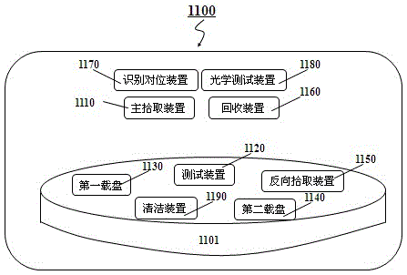
[0064] Embodiments of the present invention describe a transfer system for transferring a micro-element and a method for transferring a micro-element array using the transfer system. Among them, the micro-element array can be micro-LED devices, diodes, transistors, integrated circuit (IC) chips, etc., and its size can be 1-5000 μm, but it is not necessarily limited thereto, and some aspects of the embodiment can be applied to larger and larger smaller size.

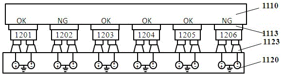
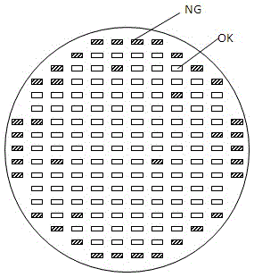
[0065] The transfer system has a main picker for picking up or releasing micro components, the main picker has a series of arrays of picker units, each picker unit has a size (eg length or width) of 1 to 5000 μm, for example 10 to 100 μm, or 100 ~500 microns, or 1000 ~5000 microns. The transfer system is also provided with a test device, which has a test circuit and a test platform. A series of test electrodes are arranged on the surface of the test platform. The electrode of the component is in contact with the test el...


PUM

PropertyMeasurementUnit
Sizeaaaaaaaaaa

Abstract

The present invention provides a transfer system and transfer method of microelements, a manufacturing method, a device and an electronic device. The transfer system of the microelements comprises a main pick-up device, a test device, a first carrying disc and a second carrying disc; the main pick-up device is used for picking up or releasing the microelements; the test device is provided with a test platform and a series of test circuits; the surface of the platform is provided with a series of test electrodes which are connected with the test circuits; the first carrying disc is used for carrying an original microelement array; and the second carrying disc is used for carrying a receiving substrate. When the transfer system is adopted to transfer the microelements, the main pick-up device is adopted to pick up the microelements and move the microelements to the platform of the test device; the test device is adopted to test the microelements; and qualified microelements picked up by the main pick-up devices are released onto the receiving substrate according to test results.

Description

technical field [0001] The present invention relates to a micro-element for display, and more particularly, to a transfer device, a transfer method, a manufacturing method, a device and an electronic device for a micro-element. Background technique [0002] Micro-component technology refers to an array of micro-sized components integrated at high density on a substrate. At present, micro-pitch light-emitting diode (Micro LED) technology has gradually become a research hotspot, and the industry expects high-quality micro-component products to enter the market. High-quality fine-pitch light-emitting diode products will have a profound impact on traditional display products such as LCD / OLED that are already on the market. [0003] In the process of fabricating microcomponents, the microcomponents are first formed on a donor substrate and then transferred to a receiving substrate. The receiving substrate is, for example, a display screen. One difficulty in the fabrication of ...

Claims


Application Information

Patent Timeline
IPC IPC(8): H01L21/677B81C1/00B81C3/00
CPCH01L21/67763B81C1/00015B81C1/00349B81C3/008H01L22/12H01L22/14H01L22/20H01L21/6835H01L2221/68368H01L2221/68354H01L2221/68322H01L2221/68381B81C99/002H01L21/67259H01L21/6838H01L22/34G01R31/00
Inventor 徐宸科邵小娟郑建森梁兴华其他发明人请求不公开姓名
Owner XIAMEN SANAN OPTOELECTRONICS TECH CO LTD
Why Eureka
Try Eureka